


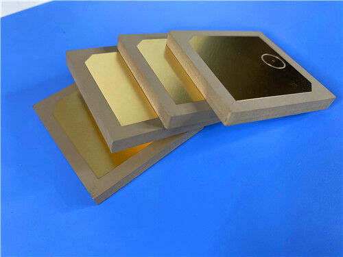
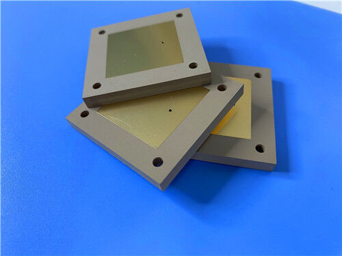
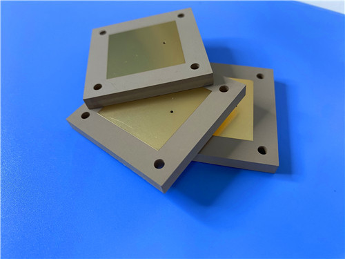
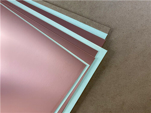
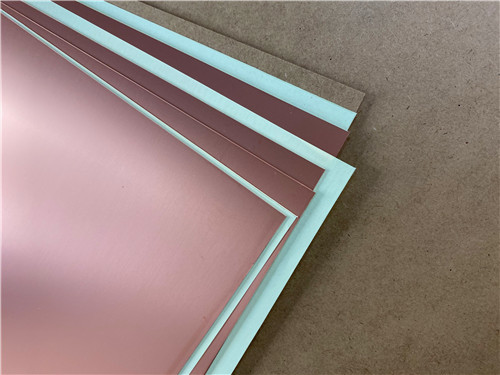

Low Loss Printed Circuit Board (PCB) on TU-883 Substrate and TU-883P Prepreg Multi-layer TU-883 PCB
Contact Person : Sally Mao
Phone Number : 86-755-27374847
WhatsApp : +8618277967574
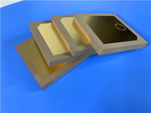
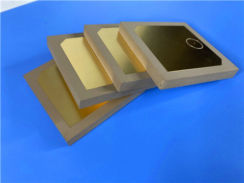
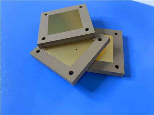
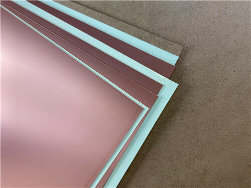
| Brand Name: | Wangling | Model Number: | TP2200 |
|---|
Product Description
When miniaturization is the driving requirement—whether for a BeiDou navigation antenna, a missile-borne seeker, or a fuze assembly—the dielectric constant of the substrate becomes a powerful design lever. The higher the Dk, the smaller the resonant element can be. The TP2200 from Taizhou Wangling Insulation Materials Factory takes this principle to an extreme, offering a Dk of 22.0 in a thermoplastic laminate that is machinable, radiation resistant, and cost-effective compared to ceramic substrates.
TP materials are a unique class of high-frequency thermoplastic laminates. The dielectric layer of the TP series is composed of ceramic and polyphenylene oxide (PPO) resin, containing no glass fabric reinforcement. By adjusting the ratio between ceramic and PPO resin, the dielectric constant can be precisely controlled. Manufactured with a special process, the material offers excellent dielectric performance and high reliability. In this series, TP refers to unclad smooth material, TP-1 refers to single-sided copper clad, and TP-2 refers to double-sided copper clad.
Key Properties at a Glance (TP2200):
| Property | Typical Value | Test Condition |
| Dielectric Constant (Dk) | 22.0 ± 0.88 (±4%) | 5 GHz |
| Dissipation Factor | 0.0020 – 0.0025 | 5 GHz |
| Dielectric Constant Temperature Coefficient | -55 ppm/°C | -55°C to +150°C |
| CTE - X / Y / Z | 35 / 35 / 40 ppm/°C | -55°C to +150°C |
| Thermal Conductivity | 0.90 W/m·K | Z-direction |
| Moisture Absorption | ≤0.01% | 20±2°C, 24 hours |
| Density | 2.77 g/cm³ | Room temperature |
| Long-Term Operating Temperature | -100°C to +150°C | — |
| Copper Foil Type | ED Copper | 0.018mm, 0.035mm |
Note: Dk can be customized from 3.0 to 25. Common values include 3.0, 4.4, 6.0, 6.15, 9.2, 9.6, 10.2, 11, 16, and 20. When Dk ≤ 10.2, the minimum thickness is 0.5mm; when Dk > 10.2, the minimum thickness is 0.8mm.
| PCB Capability (TP Series) | |||
| PCB Material: | Polyphenylene ether, ceramic | ||
| Designation (TP Series) | Designation | DK | DF |
| TP300 | 3.0±0.06 | 0.0010 | |
| TP440 | 4.4±0.09 | 0.0010 | |
| TP600 | 6.0±0.12 | 0.0010 | |
| TP615 | 6.15±0.12 | 0.0010 | |
| TP920 | 9.2±0.18 | 0.0010 | |
| TP960 | 9.6±0.2 | 0.0011 | |
| TP1020 | 10.2±0.2 | 0.0011 | |
| TP1100 | 11.0±0.22 | 0.0011 | |
| TP1600 | 16.0±0.32 | 0.0015 | |
| TP2000 | 20.0±0.4 | 0.0020 | |
| TP2200 | 22.0±0.44 | 0.0022 | |
| TP2500 | 25.0±0.5 | 0.0025 | |
| Layer count: | Single Sided, Double Sided PCB | ||
| Copper weight: | 1oz (35µm), 2oz (70µm) | ||
| Dielectric thickness (Dielectric thickness or overall thickness) | 0.5mm, 0.8mm, 1.0mm, 1.2mm, 1.5mm, 2.0mm, 3.0mm, 4.0mm, 5.0mm, 6.0mm, 7.0mm, 8.0mm, 10.0mm, 12.0mm | ||
| PCB size: | ≤150mm X 220mm | ||
| Solder mask: | Green, Black, Blue, Yellow, Red etc. | ||
| Surface finish: | Bare copper, HASL, ENIG, Immersion silver, Immersion tin, OSP, Pure gold, ENEPIG etc.. | ||
Applications
Custom PCB Manufacturing on TP2200
As a specialized manufacturer of high-frequency printed circuit boards, we offer comprehensive fabrication services using TP2200 and other advanced materials. The following specification details a representative 2-layer rigid PCB implementation:
PCB Construction Details:
| Parameter | Specification |
| Base Material | TP2200 |
| Layer Count | 2-layer rigid |
| Board Dimensions | 35.65mm × 87mm per panel, ±0.15mm |
| Finished Thickness | 10.9mm |
| Copper Weight | 1 oz (1.4 mils) outer layers |
| Minimum Trace/Space | 4 / 7 mils |
| Minimum Hole Size | 0.4mm |
| Via Structure | No blind or buried vias |
| Via Plating Thickness | 20 μm |
| Surface Finish | Immersion Gold |
| Solder Mask | None (bare substrate) |
| Silkscreen | None |
| Electrical Test | 100% prior to shipment |
| Artwork Format | Gerber RS-274-X |
| Quality Standard | IPC-Class-2 |
With a Dk of 22.0 ± 0.88 at 5 GHz, TP2200 enables dramatic miniaturization of resonant structures. For patch antennas and other frequency-selective elements, the physical size scales inversely with the square root of Dk—meaning a Dk of 22 allows an element roughly one-quarter the size of an equivalent Dk 2.2 design. The Dk can be customized from 3.0 to 25 to suit specific design requirements.
A dissipation factor of 0.0020–0.0025 at 5 GHz is remarkably low for a material with such a high dielectric constant, ensuring acceptable efficiency even in miniaturized antennas.
Unlike ceramic substrates, TP2200 is easily machined—it can be drilled, turned, milled, sheared, and engraved. This is a significant advantage over alumina and other ceramic substrates, which are brittle and difficult to machine. The material processes like a standard thermoplastic, yielding high production yields and significantly lower processing costs than ceramic alternatives.
Copper foil adhesion to the TP2200 dielectric is more reliable than vacuum-deposited films on ceramic substrates, ensuring robust circuit integrity through handling and assembly.
TP2200 is resistant to radiation and exhibits low outgassing, making it suitable for space, missile, and other high-reliability applications.
The dielectric constant temperature coefficient of -55 ppm/°C over -55°C to +150°C provides stable performance across temperature. The CTE of 35/35/40 ppm/°C in X/Y/Z is reasonably matched to copper, supporting plated through-hole reliability. Long-term operating temperature ranges from -100°C to +150°C.
At ≤0.01%, TP2200 absorbs virtually no moisture, ensuring stable electrical properties even in humid environments.
A thermal conductivity of 0.90 W/m·K in the Z-direction aids heat dissipation, important for high-power miniaturized circuits.
TP2200 is a thermoplastic material with specific processing requirements that differ from thermoset laminates:
Soldering: The material is not suitable for 260°C thermal shock testing and cannot be wave soldered. Soldering is recommended using a constant-temperature soldering iron for manual assembly. Reflow soldering is generally not recommended; if performed, the maximum set temperature should not exceed 200°C, with full consideration of feasibility and stability.
Multilayer Construction: Due to the material's characteristics, multilayer processing is generally not recommended. If multilayer construction is required, low-temperature bonding prepregs should be selected, and feasibility should be fully evaluated.
Machining: The material can be drilled, turned, milled, sheared, and engraved using standard thermoplastic machining methods.
Quality and Availability
All boards are manufactured in compliance with IPC-Class-2 quality standards, ensuring robust reliability for commercial, industrial, and defense-related applications. 100% electrical testing is performed prior to shipment to guarantee functional integrity.
Our production capability extends to worldwide availability, with flexible shipping and logistics support for both prototype and volume requirements. We offer rapid turnaround and competitive pricing while maintaining strict process control.
For inquiries about custom stack-ups, panel sizes, alternative Dk values within the TP series (3.0 to 25), single- or double-sided copper cladding, or other configurations, please contact our sales engineering team—we are ready to support your high-frequency circuit board requirements.
Enter Your Message

RO4350B, 4003C; Rogers 5880, 5870, 6002, 6010, 6006, 6035; RO3003, RO3035, RO3006, RO3010, RO3210,RO3203
TLX-8, TLX-6, TLX-9, TLX-0, TLX-7, TLY-3, TLY-5, RF-35TC, RF-60TC, RF-35A2, RF-60A, AD450, AD600, TMM4, TC350
| Shenzhen Bicheng Electronics Technology Co., Ltd |
| 6-11C Shidai Jingyuan Fuyong Town, Baoan District, Shenzhen City, Guangdong Province, China |
| 86-755-27374946 |
| sales30@bichengpcb.com |