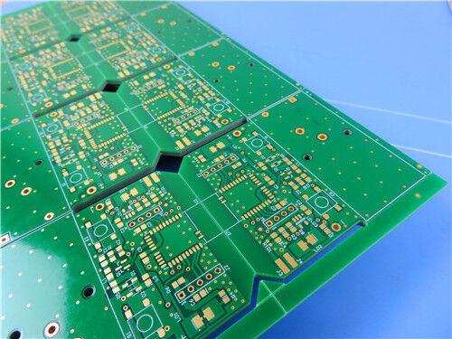
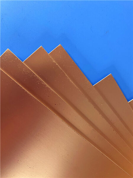
logo
Hot Products Top Products
About Us
China Shenzhen Bicheng Electronics Technology Co., Ltd
About Us
Shenzhen Bicheng Electronics Technology Co., Ltd
Founded in 2003, Shenzhen Bicheng Electronics Technology Co., Ltd. has established itself as a reliable high-frequency PCB supplier and exporter based in Shenzhen, China. For over 24 years, we have served industries worldwide, including cellular base station antennas, satellite communications, high-frequency passive components, microstrip and strip line circuits, millimeter-wave equipment, radar systems, and digital RF antennas. Our high-frequency PCBs are primarily manufactured using three ...
Read more
Request A Quote
0+
Annualsales
0
Year
0%
P.C
0+
Employees
WE PROVIDE
THE BEST SERVICE!
You can contact us in various ways
Contact Us
Shenzhen Bicheng Electronics Technology Co., Ltd

quality Bicheng Newly shipped PCB & Rogers PCB Board factory

Events
Lastest company news about [Hot Topic] Why are semiconductor material prices rising again? Let's find out.
[Hot Topic] Why are semiconductor material prices rising again? Let's find out.

2026-05-22

Recently, Japanese semiconductor materials supplier Sumitomo Bakelite announced a price increase for its "epoxy molding compound (EMC) for semiconductor devices."   The price increase covers all grades of Sumitomo Bakelite's EMC for packaging, with increases ranging from 10% to 20%, effective June 1, 2026. Sumitomo Bakelite holds approximately 40% of the global market share in semiconductor EMC, with products covering both traditional and advanced packaging needs, applicable to automotive electronics, industrial modules, and data centers.   Regarding the reason for the price adjustment, Sumitomo Bakelite stated that the recent situation in the Middle East has led to increased procurement costs for raw materials used in its EMC. Furthermore, rising costs for packaging materials, energy, and transportation have further increased the overall product cost. This is not the first time EMC prices have increased. In early April, Kumho Petrochemical of South Korea and Mitsubishi Chemical of Japan issued price increase notices for engineering plastics such as EMC, with increases ranging from a minimum of 5% to a maximum of 20%. Epoxy resin film plastics are thermosetting molding compounds made by compounding epoxy resin as a matrix with curing agents, inorganic fillers, and various additives.   They are widely used in the semiconductor packaging field to protect chips from external environmental influences and provide electrical insulation and heat dissipation. The price surge in epoxy resin molding compounds ultimately stems from supply disruptions to raw materials such as resin. According to Nikkei, the closure of the Strait of Hormuz has led to severe supply shortages of methanol, xylene, and related solvents, with prices rising by at least 40% since March. These solvents are essential raw materials for the production of various specialty resins.   The rising prices of resins and their raw materials are impacting all aspects of the semiconductor and PCB industry chain: an executive at a chip substrate supplier stated that Mitsubishi Gas Chemical has already raised the prices of some products by 20% in the first quarter of this year. He added that given the overall rising material costs, CCL prices are expected to rise further.   Huafu Securities points out that electronic resin, as the core substrate of copper-clad laminates, is crucial in determining the signal transmission efficiency and reliability of the board. Its industry chain extends from upstream resin synthesis through prepreg processing to downstream PCB conduction. Against the backdrop of explosive growth in AI computing power, computing chips are demanding signal transmission speeds exceeding 224Gbps, forcing PCB materials to leap from traditional FR-4 to M8, M9, and even higher-level high-frequency, high-speed copper-clad laminates. The core driving force lies in the iterative upgrades of resin systems. Affected by escalating geopolitical conflicts in the Middle East and disruptions to shipping through the Strait of Hormuz, costs across the petrochemical industry chain have risen across the board, leading to significant increases in the prices of various commodities. The upstream suppliers of core CCL materials such as epoxy resin and PPO resin are also largely petrochemical companies. With raw material costs continuing to rise, price increases are expected to intensify.       =================================================================================== Copyright statement: The copyright of the information in this article belongs to the original author and does not represent the views of this platform. It is for sharing only. If there are copyright and information errors involved, please contact us to correct or delete it. Thanks!
View More
Lastest company news about Middle East Conflict Disrupts Raw Material Supply, Driving Up PCB Prices
Middle East Conflict Disrupts Raw Material Supply, Driving Up PCB Prices

2026-05-13

Industry executives warn of soaring costs for resins, copper, and glass fiber, impacting everything from smartphones to AI servers.   The ongoing conflict in the Middle East is severely disrupting the supply of key raw materials, driving up the prices of printed circuit boards (PCBs) used in nearly all electronic devices — from smartphones and computers to advanced AI servers, according to industry executives and insiders. This new disruption adds further pressure on electronics manufacturers already grappling with soaring memory chip costs. It also highlights the widening impact of the conflict, which has already disrupted global supply chains, plastics, and oil supplies. In early April, an attack on a petrochemical complex in Jubail, Saudi Arabia, halted the production of high-purity Polyphenylene Ether (PPE) resin — a critical base material for manufacturing PCB laminates. According to a source, Saudi Basic Industries Corporation (SABIC), which supplies approximately 70% of the world’s high-purity PPE, operates the Jubail facility. Production has yet to resume, causing a severe global supply shortage of the material. The conflict has also significantly disrupted shipping routes in the Gulf region. PCB prices had already been climbing since late last year, driven by growing demand for AI servers. Three industry insiders say that demand has accelerated sharply since March, as manufacturers scramble to secure raw material supplies and mitigate cost surges. In a recent report, Goldman Sachs analysts noted that PCB prices jumped 40% in April alone compared to March. They added that cloud service providers are accepting further price increases, anticipating that demand will outpace supply for the foreseeable future. According to a recent report by Prismark, the global PCB industry is expected to grow by 12.5% to reach $95.8 billion by 2026. An executive at Daeduck Electronics — a South Korean PCB manufacturer whose clients include Samsung Electronics, SK Hynix, and AMD — told Reuters that the company has begun discussing price increases with customers. Speaking on condition of anonymity due to the sensitivity of the matter, the executive said his focus has now shifted from meeting clients to communicating with suppliers, as lead times for chemical materials like epoxy resin have extended from 3 weeks to as long as 15 weeks. The sharp rise in PCB prices is also due to shortages of other key materials, including fiberglass and copper foil. According to one source, copper foil prices have surged as much as 30% this year, with the acceleration picking up in March. Copper accounts for approximately 60% of the total raw material cost of PCB manufacturing, according to Shenzhen Hongxin Electronics Technology, a major Chinese PCB supplier to Nvidia. The Chinese company warned earlier this month that the Middle East conflict could drive up prices for key materials, including resin and copper. According to Shenzhen Hongxin, a standard multi-layer PCB now costs approximately 1,394 yuan per square meter, while high-end models used for AI servers cost around 13,475 yuan per square meter. Bicheng is a leading provider of custom PCB solutions. We closely monitor global supply chain trends to help our customers navigate market challenges and deliver high-quality, reliable boards for every application. Visit our website to learn more about our custom PCB services and current lead times.     =================================================================================== Copyright statement: The copyright of the information in this article belongs to the original author and does not represent the views of this platform. It is for sharing only. If there are copyright and information errors involved, please contact us to correct or delete it. Thanks!  
View More
Lastest company news about How much do you know about copper clad laminate (CCL)? Let me explain.
How much do you know about copper clad laminate (CCL)? Let me explain.

2025-09-10

How much do you know about copper clad laminate (CCL)? Let me explain.   Copper clad laminate (CCL) is the core substrate for PCBs, with downstream applications in communications, computers, automotive, industrial, and medical fields. Its upstream suppliers include raw materials such as copper foil, resin, and glass fiber, while its downstream suppliers include PCB manufacturers and end-use electronic product manufacturers. This industry is highly cyclical and is entering a new growth cycle, driven by emerging demands such as 5G, AI servers, and automotive electronics.     CCL is a sheet material made by hot-pressing a reinforcing material impregnated with resin, coated on one or both sides with copper foil, and then hot-pressed. It fulfills the three main functions of conducting electricity, insulating, and supporting printed circuit boards, making it a core material for PCB manufacturing.     The CCL industry chain has a clear three-tier structure: upstream raw material supply (copper foil, glass fiber cloth, resin, filler, etc.), midstream CCL manufacturing, and downstream PCB applications.     The three core raw materials for CCL are copper foil, resin, and glass fiber cloth, accounting for 42%, 26%, and 19% of the cost, respectively, for a total of 87%.   If you require additional substrates, please feel free to contact us! Bicheng Company specializes in providing high-frequency circuit boards and raw materials.  
View More
Lastest company news about [Hotspot] Global PCB output value grows steadily, and AI capital expenditure heats up the underlying material track
[Hotspot] Global PCB output value grows steadily, and AI capital expenditure heats up the underlying material track

2025-07-16

On July 8, the PCB concept was hot. According to Prismark statistics, the global PCB output value is expected to grow to US$94.7 billion in 2029. The CAGR from 2024 to 2029 will reach 5.2%; the PCB output value of the Chinese market will reach US$49.7 billion in 2029.     In addition, in 2025, the capital expenditure of cloud factories such as Microsoft and Google will increase by more than 30% year-on-year. The capital expenditure of China's Alibaba and Tencent is expected to exceed 120 billion/80 billion yuan, and the demand for AI infrastructure will drive the accelerated expansion of the production capacity of underlying materials such as PCB.     The AI-driven technological innovation upcycle will last longer and generate greater market demand. China's PCB industry continues to upgrade and expand mid-to-high-end production capacity and deploy overseas production capacity, and its performance release is sustainable.     The overall demand for downstream electronics is currently showing a recovery trend, coupled with the continued upward momentum in innovative fields represented by AI and high-speed communications, which together support the growth in overall PCB demand. With the iteration of AI hardware performance, PCB will be further upgraded to higher specifications in terms of product technology and materials. Relying on its early technological accumulation and improved product competitiveness, Bicheng Technology has gradually improved its industry position in the high-end market, and its AI PCB supply share has continued to increase. Bicheng is expected to achieve rapid development by seizing the opportunities of AI development.       =================================================================================== Copyright statement: The copyright of the information in this article belongs to the original author and does not represent the views of this platform. It is for sharing only. If there are copyright and information errors involved, please contact us to correct or delete it. Thanks!
View More
Latest company case about An Aerospace-Grade, No-Mask RF PCB with Ceramic-Filled PTFE
An Aerospace-Grade, No-Mask RF PCB with Ceramic-Filled PTFE

2026-06-25

In the demanding world of aerospace and defense electronics, material science is not just an enabler—it is the cornerstone of performance. This case study explores a custom PCB design that pushes the boundaries of high-frequency engineering by leveraging an advanced, ceramic-filled PTFE substrate. The design's minimalist philosophy, featuring no solder mask and no silkscreen, underscores a relentless focus on signal integrity and reliability.   The Brief: A Compact Powerhouse for Critical Applications This project involved the design and fabrication of a 2-layer rigid printed circuit board with very specific performance targets. The board is compact, measuring 97.53mm x 100.28mm, yet it is built to handle some of the most demanding applications in aerospace, radar, and satellite communications.   Decoding the Bill of Materials: The "Why" Behind the "What" The specifications reveal a design where every choice is intentional, prioritizing electrical performance above all else.   The Substrate: TFA294 Ceramic-Filled PTFE The heart of this PCB is the TFA294 dielectric material, a member of the TFA series. This is not a standard PTFE laminate reinforced with glass fiber. Instead, it is a sophisticated composite where PTFE resin is filled with a high volume of uniform, specialized nano-ceramics . This innovative construction method offers several profound advantages.   The most critical benefit is the elimination of the "fiberglass effect." In traditional woven-glass PTFE laminates, the weave of the glass can create microscopic variations in the dielectric constant (Dk). At very high frequencies, these variations can impact phase consistency and signal integrity. By using a homogeneous ceramic-filled system, the TFA series provides exceptional Dk uniformity and minimal X/Y/Z anisotropy. This is critical for sensitive applications like phased array antennas and beamforming networks. Its Dk of 2.94 at 10 GHz and dissipation factor of 0.0010 make it an extremely low-loss material, crucial for minimal signal attenuation in RF and microwave circuits.   A Minimalist Design Philosophy: No Solder Mask, No Silkscreen The absence of solder mask and silkscreen on both sides of the board is the most visually striking feature. This "bare" approach is a deliberate engineering decision for the highest-frequency designs: Ultimate Signal Integrity: Solder mask, while providing protection, is an added dielectric layer with its own loss and impedance characteristics. At microwave frequencies, even these small losses can degrade performance. Removing it ensures the signal interacts only with the high-performance TFA294 substrate and the copper traces, creating a more predictable and low-loss transmission path. High-Voltage/Power Capability: The absence of a dielectric layer can also be beneficial in designs with high voltage potentials or high-power RF, where solder mask breakdown could be a concern. Simplified Manufacturing for Performance: By omitting these non-functional layers, the fabrication process is streamlined, reducing potential points of failure and focusing entirely on the critical conductor geometry.       Construction and Performance Statistics The PCB's fabrication details reinforce its precision and performance-oriented design: Board Dimensions: 97.53mm x 100.28mm with a tight tolerance of +/- 0.15mm, indicating a requirement for precise mechanical fit and alignment in a larger system. Stackup: A 2-layer construction with 35 μm (1 oz) copper on both sides of a 1.016 mm (40 mil) TFA294 core. Trace/Space: A fine-pitch minimum of 4/6 mils allows for dense, controlled-impedance routing within the board's area. Surface Finish: Immersion Gold (ENIG) provides an excellent, flat, solderable surface for the 14 top-side SMT pads, ensuring reliable solder joints for sensitive components . Testing: A 100% electrical test prior to shipment is a mandatory step to guarantee that the careful design and specialized materials translate into a fully functional product.         The Design Decisions: A Closer Look Examining the component and network structure reveals a focused, high-performance sub-system. The board contains 21 components, a modest number that includes 18 through-hole pads and 14 SMT pads. The presence of 13 vias provides a compact routing solution. The fact that the board has only 2 nets is its most telling feature. This stark simplicity is not a limitation but a direct clue to its application.   A design with only two nets is highly specialized. It is likely a high-power or high-frequency sub-circuit, such as: An RF Coupler or Filter: These devices often have very few connections (input, output, and ground). A Power Amplifier (PA) Sub-Section: A transistor-based amplifier might have a few DC bias networks but is fundamentally a "2-net" RF path. An Antenna Feed Network: A balun or a simple impedance transformer would have a similar structure.     Its acceptance to the IPC-Class-2 standard is significant. While Class-3 is for high-reliability life-support equipment, Class-2 represents a "dedicated service electronic product" with a high level of reliability, which is often the sweet spot for aerospace and defense sub-assemblies where performance and cost-effectiveness are both critical.     Conclusion: A Masterclass in Application-Specific Design This custom PCB is a perfect example of how material selection, in conjunction with a minimalist design philosophy, delivers unmatched performance for a specific application. By choosing the aerospace-grade TFA294 material, the designer ensured an optimal foundation for high-frequency performance, free from the anomalies of traditional woven-glass materials. The decision to omit solder mask and silkscreen is a testament to the designer's deep understanding of how to minimize parasitic losses and preserve signal fidelity at microwave frequencies.   This board is not a generic product; it is a purpose-built solution designed to excel in the harsh and demanding environment of aerospace and radar systems. It is a small, unassuming component that plays a critical role in the larger, sophisticated systems it serves—a true reflection of the power of purposeful engineering.
View More
Latest company case about A Deep Dive into a High-Performance, No-Mask RF DiClad 527 PCB Design
A Deep Dive into a High-Performance, No-Mask RF DiClad 527 PCB Design

2026-06-23

In the world of high-frequency electronics, the mantra is often "less is more." When signal integrity is paramount, every material choice, every design decision, and every manufacturing process must be meticulously scrutinized. This is the story of a fascinating custom PCB project that embodies this principle, leveraging the advanced properties of a specialized substrate to create a robust, high-performance two-layer board.   The Brief: A Foundation for High-Frequency Excellence This project centered around the design and fabrication of a 2-layer rigid printed circuit board. At its heart lay a specific material: Rogers DiClad 527. This wasn't a standard FR-4 design; it was a board built from the ground up to excel in demanding RF and microwave applications.   Decoding the Bill of Materials: The "Why" Behind the "What" The specifications of this PCB reveal a clear design philosophy centered on performance, precision, and reliability for high-frequency signals.     The Substrate: Rogers DiClad 527 The most critical choice was the base material. Unlike standard FR-4, DiClad 527 is a PTFE (Teflon) composite reinforced with woven fiberglass. This is a classic material family for high-frequency work because PTFE has inherently low signal loss .   What makes the *527* variant special is its higher ratio of fiberglass reinforcement. This gives it superior dimensional stability compared to some other PTFE materials. Its key properties at 10 GHz are a stable Dielectric Constant (Dk) between 2.40 and 2.60 and an exceptionally low Dissipation Factor (Df) of 0.0017 . For an engineer, this means predictable impedance, minimal signal attenuation, and consistent performance across a wide frequency range.   A Minimalist Design Philosophy: No Solder Mask One of the most striking features of this PCB is the complete absence of solder mask on both the top and bottom layers. For those used to seeing ubiquitous green (or black, red, blue) boards, this might seem strange. However, it is a deliberate choice for high-frequency designs:   Signal Integrity: Solder mask has a dielectric constant and a dissipation factor of its own. At high frequencies, this material can become a source of signal loss and impedance variation. By removing it, the signal travels in a more controlled, consistent environment, primarily interacting only with the high-performance DiClad substrate and copper. High-Voltage Applications: The absence of a dielectric layer can also be beneficial in designs with high voltage potentials or high-power RF, where solder mask breakdown or arcing could be a concern.       Construction and Performance Statistics The PCB’s fabrication details further reinforce its performance-oriented design: Board Dimensions: 49.63mm x 91.54mm with a tight tolerance of +/- 0.15mm, indicating a need for precise mechanical fit. Stackup: A classic 2-layer construction with 35 μm (1 oz) copper on both sides of a 0.508 mm (20 mil) DiClad core. Trace/Space: A minimum of 4/6 mils, demonstrating the need for fine-feature routing to accommodate the 36 components and 104 pads within the compact board area . Surface Finish: Immersion Gold (ENIG) provides a flat, solderable surface, which is excellent for the 41 top-side SMT pads, and also offers corrosion resistance . Testing: A 100% electrical test prior to shipment ensures that the careful design and specialized materials translate into a fully functional product.       The Design Decisions: A Closer Look Let's examine the component and network structure. The board contains 36 components, 104 total pads (63 of which are through-hole), and 19 vias. This is a mixed-technology design, leveraging the mechanical strength of through-hole components and the density of SMT. The fact that the board has only 2 nets is particularly interesting. This stark simplicity suggests the board is a very specific, potentially high-power or high-frequency sub-circuit—like a filter, a balun, a coupler, or a simple antenna feed network—rather than a complex, multi-function digital board .   The IPC-Class-2 standard acceptance means the board is designed for dedicated service electronic products, a level of reliability that fits this kind of application perfectly.     Conclusion: A Masterclass in Material-Driven Design This custom PCB is a brilliant example of how material selection drives the entire design process. By choosing Rogers DiClad 527, the designer ensured the board had an optimal foundation for high-frequency performance. The decision to forgo solder mask, a seemingly minor detail, reveals a deep understanding of how parasitic losses can degrade a signal. The precise construction, including the specific copper weight, plating thickness, and tight tolerances, demonstrates a commitment to producing a reliable, high-yield product.     This board isn't just a collection of components on a substrate; it's a testament to the power of purposeful engineering—a device where every material and specification is chosen to fulfill a specific, high-performance mission.
View More
Latest company case about A 2-Layer Wangling TP440 High-Frequency PCB for Miniaturized Antenna Applications
A 2-Layer Wangling TP440 High-Frequency PCB for Miniaturized Antenna Applications

2026-06-18

A 2-Layer Wangling TP440 High-Frequency PCB for Miniaturized Antenna Applications     Introduction In the world of RF and microwave design, material selection is arguably the most critical decision an engineer can make. For applications demanding specific dielectric constants, exceptional stability, and reliability in harsh environments, standard FR-4 materials simply won't suffice. This case study examines a custom PCB built on Wangling TP440 material, a unique high-frequency thermoplastic with a dielectric constant (Dk) of 4.4, designed for demanding antenna applications. This board illustrates the capabilities of the TP series, particularly its ability to enable circuit miniaturization without sacrificing performance.     Project Overview & Technical Specifications This project involved the design of a compact, 2-layer rigid PCB measuring 67.5mm x 58.6mm. The board is characterized by its minimalist design, featuring only 11 components, 19 pads, and a single net, underscoring the highly specialized nature of its function. The design's simplicity is a testament to the efficiency of the chosen material; the inherent properties of the TP440 core allow for a straightforward, yet high-performance circuit.     The full construction details are as follows: Base Material: Wangling TP440 (a ceramic-filled Polyphenylene Oxide resin composite) . Layer Count: 2-layer rigid PCB. Board Dimensions: 67.5mm x 58.6mm, +/- 0.15mm. Minimum Trace/Space: 6/8 mils. Minimum Hole Size: 0.3mm. Blind Vias: No. Finished Board Thickness: 0.6mm. Finished Cu Weight: 1oz (35 μm) outer layers . Via Plating Thickness: 20 μm. Surface Finish: Immersion Gold (ENIG). Silkscreen & Solder Mask: None. Quality Standard: IPC-Class-2. 100% Electrical Test: Used prior to shipment .     The Core Material: Wangling TP440 The PCB's performance hinges on its core material, Wangling TP440. This material is part of a unique series of high-frequency thermoplastics that set it apart from conventional PCB substrates. Unlike standard materials reinforced with fiberglass, TP440's dielectric layer is composed of a precise blend of ceramics and PPO resin .     The defining feature of the Wangling TP series is its tunable dielectric constant (Dk) . By adjusting the ratio of ceramic to PPO resin, the Dk can be customized within a range of 3 to 25 . The TP440 variant is specified to have a Dk of 4.4 ± 0.09 and a low dissipation factor (Df) of 0.0010 at 10 GHz, ensuring minimal signal loss at high frequencies . This precise, stable Dk and ultra-low loss are crucial for applications where signal integrity is paramount .     Key Advantages for Demanding Applications The choice of TP440 material for this PCB was driven by several key requirements typical of advanced antenna systems:   Miniaturization: For a given frequency, the physical size of a circuit element like a patch antenna is inversely proportional to the square root of the dielectric constant . A higher Dk allows for a significantly smaller antenna design. The TP440's Dk of 4.4 enables a more compact form factor compared to standard materials (like FR-4 with a Dk of ~4.3-4.5) while maintaining superior high-frequency performance.     High-Frequency Stability: The TP material maintains its low dielectric loss across a wide frequency range, up to and beyond 10 GHz. This stability is essential for consistent performance in applications like GPS, satellite communications, and other RF systems .     Environmental Resilience: The board is designed for reliability in extreme environments. The TP440 material boasts a long-term operating range from -100°C to +150°C, making it suitable for aerospace, military, and other outdoor applications. It is also resistant to radiation and exhibits low outgassing, a critical property for vacuum environments .     Superior Machinability: While offering performance comparable to, or better than, fragile ceramic substrates, TP material is much easier to machine. It can be processed using standard methods like drilling, etching, and shearing, avoiding the costly and complex handling required for ceramics .     Design for Manufacturing (DFM) and Reliability This PCB was fabricated with stringent quality control measures. The manufacturing process adhered to the IPC-Class-2 standard, ensuring high reliability in commercial and industrial environments. The decision to omit solder masks and silkscreens is likely to prevent any disruption to the high-frequency signal path or for size constraints, a common practice in minimalist RF designs. The use of Immersion Gold (ENIG) surface finish provides a flat, solderable surface with excellent corrosion resistance and low contact resistance, ideal for RF applications. To guarantee functionality, the board underwent a 100% electrical test before shipment .     Conclusion This custom PCB design is a prime example of how leveraging advanced materials like Wangling TP440 enables engineers to push the boundaries of high-frequency circuit design. By utilizing a material with a stable, low-loss dielectric constant and extreme environmental resilience, this compact PCB is primed for use in critical applications such as GPS antennas, Beidou navigation systems, missile-borne electronics, and miniaturized antennas . The success of this project highlights the importance of selecting the right substrate to meet the unique challenges of RF and microwave engineering.  
View More
Latest company case about Thick, Tough, and Low Loss: The WL-CT440 30mil PCB
Thick, Tough, and Low Loss: The WL-CT440 30mil PCB

2026-05-26

Thick, Tough, and Low Loss: The WL-CT440 30mil PCB Need a high-frequency board that's thicker than usual but still easy to fabricate? Meet the WL-CT440 30mil ENIG PCB. This 2-layer board (89mm x 63.5mm) is built on Wangling's WL-CT440—a thermosetting hydrocarbon-ceramic composite that bridges the gap between PTFE performance and FR-4 processability.   Why you want it: FR-4 Friendly: Unlike finicky PTFE materials, WL-CT440 processes using standard FR-4 fabrication techniques. No special via prep. Lower cost, faster turnaround. Solid RF Performance: Dielectric constant of 4.1 and dissipation factor of 0.004 at 10 GHz. Plenty for microwave and antenna work. Thick Core: At 0.8mm (30mil) finished thickness, this board offers mechanical rigidity that thinner RF laminates can't match. Stable as a Rock: TCDK of -21 ppm/°C means your Dk won't drift with temperature. CTE closely matched to copper (X: 14ppm, Y: 18ppm). No Mask, No Silkscreen: Just bare laminate, copper, and ENIG. Clean and simple.   The Specs Snapshot: Stackup: 2-Layer | 35µm copper / 0.762mm (30mil) WL-CT440 / 35µm copper Finish: Immersion Gold (ENIG) Traces/Holes: 4/6 mil trace/space | 0.2mm min hole size (tight!) Stats: 37 components, 49 pads, 31 vias Quality: IPC-Class-2 | 100% electrical test   Key Properties: Thermal Conductivity: 0.66 W/m/K (good heat dissipation) Moisture Absorption: 0.12% (low) High Tg: >280°C   Best For: Aerospace equipment, airborne radar, phased array antennas, satellite communication, power amplifiers, and navigation systems.   The Bottom Line: If you want PTFE-like RF performance without PTFE's fabrication headaches, the WL-CT440 delivers. It's thick, stable, low loss, and processes just like FR-4. A smart choice for aerospace and microwave applications.
View More

Shenzhen Bicheng Electronics Technology Co., Ltd
Cooperative Partners
map map 30% 40% 22% 8%
map
map
map
WHAT CUSTOMERS SAYS
Rich Rickett
Kevin, Received and tested the boards - thanks very much. These are perfect, exactly what we needed. rgds Rich
Olaf Kühnhold
Ruth, I got the PCB today, and they are just perfect. Please stay a little patience, my next order is coming soon. Kind regards from Hamburg Olaf
Sebastian Toplisek
Hi Natalie. It was perfect, I attach some pictures for your reference. And I send you next 2 projects to budget. Thanks a lot again
Daniel Ford
Kevin, Thanks, they were perfectly made, and work well. As promised, here are the links for my latest project, using the PCBs you manufactured for me:
CONTACT US AT ANY TIME!
Sitemap |  Privacy Policy | China Good Quality Bicheng Newly shipped PCB Supplier. Copyright © 2016-2026 Shenzhen Bicheng Electronics Technology Co., Ltd . All Rights Reserved.