



WL-CT350 High-Frequency Laminate: Is This FR-4 Processable, Low-Loss Material Right for Your Antenna PCB?
Contact Person : Sally Mao
Phone Number : 86-755-27374847
WhatsApp : +8618277967574
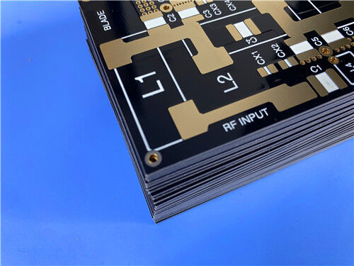
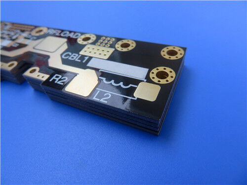
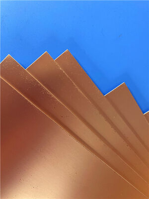
| Place of Origin: | China | Brand Name: | Wangling |
|---|---|---|---|
| Certification: | ISO9001 | Model Number: | F4BTMS450 |
Product Description
What is F4BTMS450?
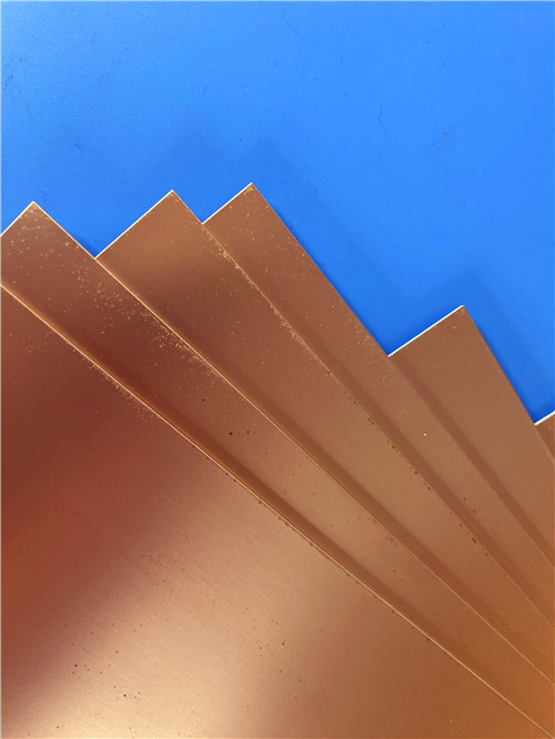
F4BTMS450 is an upgraded PTFE-based composite laminate developed by Taizhou Wangling Insulating Material Factory. It represents a technological breakthrough over the F4BTM series, incorporating a significant amount of ceramic filler with ultra-thin and ultra-fine woven fiberglass reinforcement. With a dielectric constant of 4.50 ± 0.09 at 10GHz, a dissipation factor of 0.0015 at 10GHz, and a CTE matched to copper (12 ppm/°C in X/Y), it is an aerospace-grade, high-reliability material that can replace similar imported products. The ultra-thin fiberglass minimizes the glass weave effect while enhancing dimensional stability, making it ideal for phase-sensitive applications including radar, feed networks, phased-array antennas, and satellite communications.
Key Takeaways (At a Glance)
Dk (10GHz): 4.50 ± 0.09
Dissipation Factor: 0.0015 @ 10GHz; 0.0019 @ 20GHz
TCDK (-55°C to 150°C): -58 ppm/°C
CTE (X/Y/Z): 12 / 12 / 45 ppm/°C (-55°C to 288°C)
Thermal Conductivity: 0.64 W/(m·K) – improved for higher power applications
Moisture Absorption: 0.08%
Flammability: UL 94 V-0
Electrical Strength (Z-direction): >45 kV/mm
Key Differentiator: Ultra-thin/ultra-fine fiberglass reinforcement minimizes glass weave effect while providing excellent dimensional stability
1. Why Choose F4BTMS450? – Material Selection Rationale
F4BTMS450 is the upgraded successor to the F4BTM series, featuring significant technological breakthroughs in both formulation and manufacturing processes. For engineers designing high-frequency circuits that demand both electrical performance and mechanical reliability, F4BTMS450 addresses these requirements through five key advantages:
Minimized Glass Weave Effect: Unlike traditional woven-glass PTFE laminates, F4BTMS450 uses ultra-thin and ultra-fine fiberglass cloth reinforcement. This minimizes the glass weave effect on electromagnetic wave propagation, reducing dielectric loss and decreasing X/Y/Z anisotropy. The result is more consistent impedance and phase response—critical for phase-sensitive applications like phased-array antennas.
Enhanced Dimensional Stability: The combination of ultra-thin fiberglass reinforcement with high ceramic loading provides excellent dimensional stability, ensuring tight registration during PCB fabrication and reliable performance across temperature extremes.
Superior Electrical Performance: With a Dk of 4.50 ± 0.09 and low dissipation factor (0.0015 @ 10GHz), F4BTMS450 delivers consistent electrical properties across frequency. The material maintains stable dielectric constant and low loss up to 40GHz, making it suitable for phase-sensitive applications.
Excellent Thermal Properties: The thermal conductivity of 0.64 W/(m·K) is improved over standard PTFE laminates, enabling better heat dissipation in higher-power applications. The low CTE in X/Y (12 ppm/°C) matches copper closely, ensuring reliable plated through-hole integrity.
Aerospace-Grade Reliability: With low outgassing properties meeting space application requirements, excellent radiation resistance, and stable performance from -55°C to +260°C, F4BTMS450 is qualified for demanding aerospace and defense environments.
2. Properties of F4BTMS450 Laminate
The table below consolidates all electrical, mechanical, thermal, and physical specifications for F4BTMS450 as provided in the official datasheet. All values represent typical measured data and are intended to aid in material selection.
|
— |
Test Condition | Units | Typical Value |
| Dielectric Constant (Typical) | 10 GHz, Stripline (Z-direction) | — | 4.50 |
| Dielectric Constant (Design Value) | 10 GHz, 50Ω Microstrip (Z-direction) | — | 4.5 |
| Dielectric Constant Tolerance | — | — | ±0.09 |
| Dissipation Factor (Typical) | 2 GHz | — | 0.0015 |
| Dissipation Factor (Typical) | 10 GHz | — | 0.0019 |
| Dissipation Factor (Typical) | 20 GHz | — | 0.0024 |
| Dielectric Constant Temp. Coefficient (TCDK) | -55°C to 150°C | ppm/°C | -58 |
| Peel Strength (1oz RTF copper) | — | N/mm | >1.2 |
| Volume Resistivity | Normal condition | MΩ·cm | ≥1 × 10⁸ |
| Surface Resistance | Normal condition | MΩ | ≥1 × 10⁸ |
| Dielectric Strength (Z-direction) | 5kV, 500V/s | kV/mm | >45 |
| Breakdown Voltage (X/Y-direction) | 5kV, 500V/s | kV | >54 |
| CTE – X-axis | -55°C to 288°C | ppm/°C | 12 |
| CTE – Y-axis | -55°C to 288°C | ppm/°C | 12 |
| CTE – Z-axis | -55°C to 288°C | ppm/°C | 45 |
| Thermal Stress | 260°C, 10s, 3 cycles | — | No delamination |
| Thermal Conductivity (Z-direction) | — | W/(m·K) | 0.64 |
| Long-term Operating Temperature | — | °C | -55 to +260 |
| Density | Room temperature | g/cm³ | 2.53 |
| Moisture Absorption | 20±2°C, 24 hours | % | 0.08 |
| Flammability Rating | UL-94 | — | V-0 |
| Material Composition | — | — | PTFE + Ultra-thin/ultra-fine fiberglass + Ceramic |
Test Methods Reference:
Dielectric constant (typical) is measured per GB/T 12636-1990 or IPC-TM-650 2.5.5.5 (stripline method) in the Z-direction.
Design Dk values are measured using the 50Ω microstrip method.
Other properties follow IPC-TM-650 or GBT4722-2017 standards.
All test data are typical measurement values intended to aid in material selection and do not constitute express or implied warranties.
3. Frequency & Temperature Stability
F4BTMS450 demonstrates excellent stability across both frequency and temperature:
Frequency Stability: The material maintains stable dielectric constant and low loss values from 0.5GHz to 20GHz and beyond (usable up to 40GHz), meeting design requirements across a wide frequency range.
Temperature Stability: With a TCDK of -58 ppm/°C from -55°C to 150°C, F4BTMS450 provides excellent phase stability across temperature extremes. The actual usable temperature range significantly exceeds this tested range.
4. PCB Design Case Study – From Specification to Reality
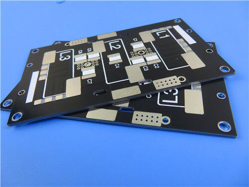
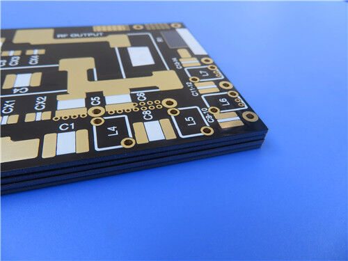
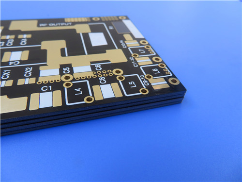
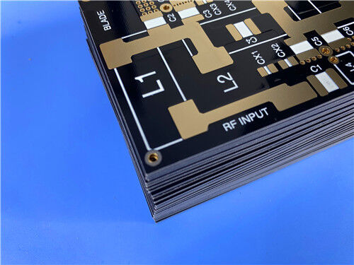
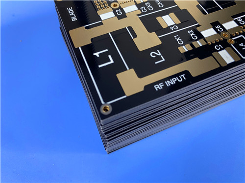
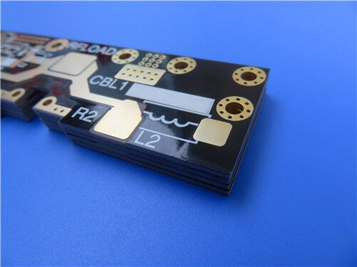
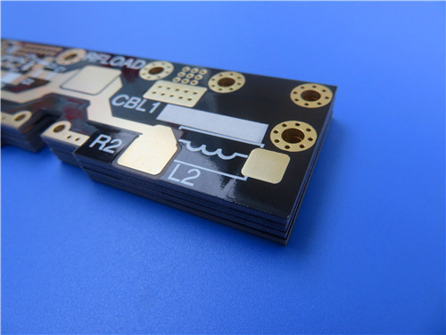
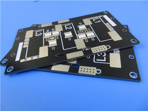
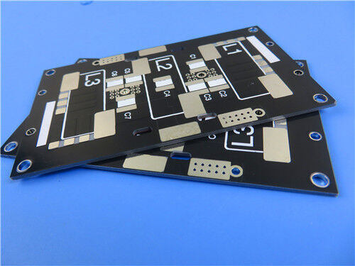
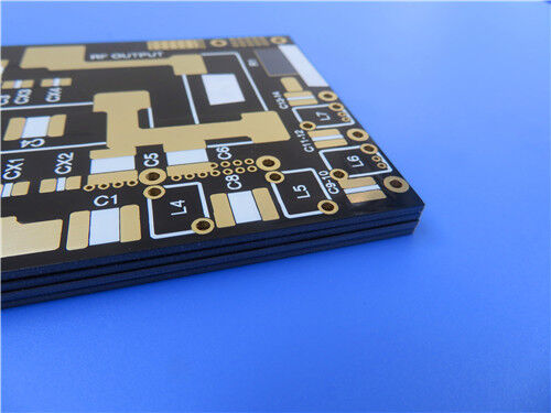
To illustrate how F4BTMS450 performs in a real-world design, here is a 2-layer board example featuring a 0.6mm finished thickness.
PCB Design Specifications
| Parameter | Specification |
| Base Material | F4BTMS450 |
| Layer Count | 2 |
| Board Dimensions | 38.4mm × 56.35mm (±0.15mm) |
| Finished Board Thickness | 0.6mm |
| PCB Stackup | Cu (35μm) / F4BTMS450 Core (0.508mm / 20mil) / Cu (35μm) |
| Minimum Trace / Space | 4 / 6 mils |
| Minimum Hole Size | 0.3mm |
| Blind Vias | None |
| Finished Copper Weight (Outer Layers) | 1oz (35μm / 1.4 mils) |
| Via Plating Thickness | 20 μm |
| Surface Finish | HASL LF (Lead-Free Hot Air Solder Leveling) |
| Top Silkscreen | White |
| Bottom Silkscreen | None |
| Top Solder Mask | Black |
| Bottom Solder Mask | None |
| Quality Standard | IPC Class-2 |
| Testing | 100% Electrical Test |
| Artwork Format | Gerber RS-274-X |
| Availability | Worldwide |
Engineering Rationale for Key Specifications:
| Parameter | Rationale |
| F4BTMS450 Selection | Chosen for its high Dk (4.50), low loss, excellent dimensional stability, and minimized glass weave effect—critical for phase-sensitive RF and radar applications. |
| 0.6mm Finished Thickness | Achieved using 20mil (0.508mm) F4BTMS450 core; provides mechanical rigidity while maintaining a compact form factor. |
| 4/6 mils Trace/Space | Fine-feature capability enabled by F4BTMS450's dimensional stability; supports dense RF and DC routing. |
| 0.3mm Minimum Hole Size | Mechanical drilling capability; no laser or blind vias required, simplifying fabrication. |
| 1oz Copper Weight | Balances current-carrying capacity with fine-feature etching capability. |
| 20 μm Via Plating | Exceeds IPC Class-2 minimum; ensures robust PTH reliability. |
| HASL LF Surface Finish | Lead-free HASL provides a solderable, cost-effective finish suitable for through-hole and SMT assembly. |
| Top Silkscreen (White) | Provides component reference designators for assembly; white offers excellent contrast on black solder mask. |
| Top Solder Mask (Black) | Protects top-side circuits; black color option per customer preference for aesthetic or optical requirements. |
| No Bottom Solder Mask | Left bare for potential grounding or heat sinking applications. |
| IPC Class-2 | Balances cost and reliability for commercial aerospace and defense applications. |
| 100% Electrical Test | Ensures impedance, continuity, and isolation before shipment. |
Key Fabrication Notes for F4BTMS450:
Drilling: F4BTMS450's ultra-thin/ultra-fine fiberglass construction requires sharp carbide drills with optimized speeds and retract rates. The fine glass reinforcement reduces tool wear compared to standard woven-glass PTFE while providing excellent hole quality.
Surface Preparation: Standard PTFE processing techniques apply. Plasma treatment (e.g., CF₄/O₂) is recommended before plating to activate the PTFE surface and ensure strong adhesion.
Dimensional Stability: The combination of ultra-thin fiberglass and ceramic filler provides excellent dimensional stability, resulting in tight registration and high fabrication yields—particularly valuable for fine-pitch designs (4/6 mils trace/space).
Solder Mask Application: Black solder mask requires careful process control for consistent color and coverage; standard PTFE-compatible solder mask formulations are recommended.
5. Comparative Positioning – How F4BTMS450 Stands Out
| Aspect | F4BTMS450 | Standard Woven-Glass PTFE | Non-Woven PTFE Laminates |
| Fiberglass Type | Ultra-thin / ultra-fine | Standard woven glass | Non-woven / chopped fiber |
| Glass Weave Effect | Minimized | Present (phase ripple) | Minimal |
| Dimensional Stability | Excellent | Good | Moderate |
| Dk @ 10GHz | 4.50 ± 0.09 | Variable | Variable |
| Dissipation Factor @ 10GHz | 0.0019 | Typically higher | Comparable |
| CTE X/Y (ppm/°C) | 12 (closely matched to Cu) | ~17–26 | Variable |
| Thermal Conductivity | 0.64 W/(m·K) | ~0.22–0.50 | ~0.20–0.50 |
| Dielectric Strength | >45 kV/mm | Lower | Comparable |
| Unique Feature | Breakthrough formulation with ultra-thin fiberglass | Standard construction | Non-woven reinforcement |
Note: F4BTMS450's ultra-thin/ultra-fine fiberglass construction minimizes the glass weave effect while providing superior dimensional stability—a combination not typically available in standard woven or non-woven PTFE laminates.
6. Typical Applications – Where F4BTMS450 Shines
Aerospace Equipment: Spaceborne systems, cabin equipment, and in-flight electronics
Microwave & RF Systems: High-frequency circuits requiring stable dielectric properties
Radar & Radar: Phased-array radars, early warning systems, and airborne radar
Feed Networks: Distribution networks for antenna systems
Phase-Sensitive Antennas: Phased-array antennas and beamforming networks
Satellite Communications: Ground stations, payloads, and communication terminals
High-Power Applications: Where improved thermal conductivity (0.64 W/(m·K)) is beneficial
Q1: What is the difference between F4BTMS450 and the F4BTM series?
F4BTMS450 is an upgraded version of the F4BTM series, featuring technological breakthroughs in material formulation and manufacturing processes. It incorporates more ceramic filler with ultra-thin and ultra-fine fiberglass reinforcement, resulting in broader Dk range, lower loss, better dimensional stability, reduced anisotropy, higher electrical strength, and improved thermal conductivity.
Q2: How does F4BTMS450 minimize the glass weave effect?
By using ultra-thin and ultra-fine fiberglass cloth combined with high ceramic loading, the glass weave effect on electromagnetic wave propagation is minimized. This reduces dielectric loss and decreases X/Y/Z anisotropy, resulting in more consistent impedance and phase response.
Q3: What is the maximum operating frequency of F4BTMS450?
The material maintains stable dielectric constant and low loss up to 40GHz, making it suitable for phase-sensitive applications across a wide frequency range.
Q4: Is F4BTMS450 suitable for space applications?
Yes. It features excellent radiation resistance, low outgassing properties meeting space requirements, and stable performance from -55°C to +260°C, making it qualified for aerospace and spaceborne applications.
Q5: What dielectric thicknesses are available for F4BTMS450?
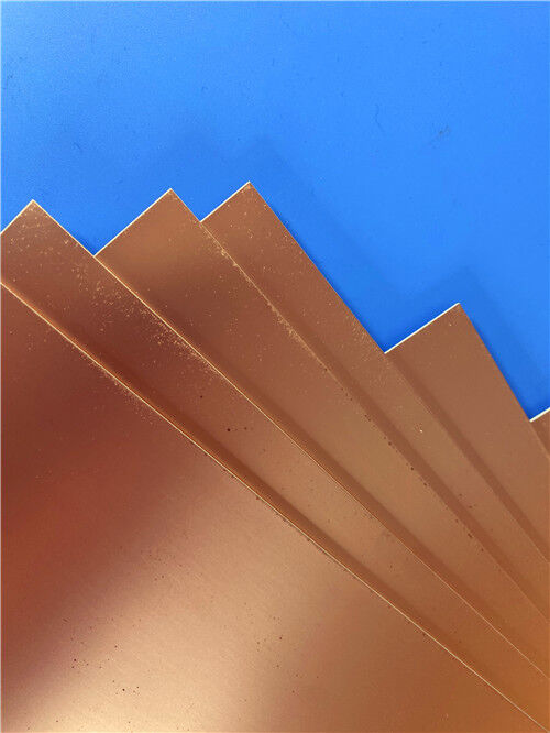
The minimum thickness is 0.254mm (10mil), with availability in 0.127mm increments up to 6.35mm (250mil). Custom thicknesses are available upon request.
Q6: Can F4BTMS450 replace imported materials?
Yes. F4BTMS450 is specifically engineered as a high-reliability alternative to similar imported products, offering comparable or superior electrical, thermal, and mechanical properties.
Q7: What surface finishes are compatible with F4BTMS450?
HASL LF (as in the design case), immersion gold, immersion silver, ENEPIG, and OSP are all compatible with proper surface preparation (plasma treatment) prior to finishing.
Q8: Are all values in the property table guaranteed?
The data provided are typical measured values intended to aid in material selection. They do not constitute express or implied warranties. End-users should verify suitability for their specific application through their own testing.
Conclusion
F4BTMS450 from Taizhou Wangling Insulating Material Factory represents a significant advancement in PTFE-based high-frequency laminates. Its innovative combination of ultra-thin/ultra-fine fiberglass reinforcement with high ceramic loading delivers minimized glass weave effect, excellent dimensional stability, and superior electrical performance—all critical attributes for phase-sensitive radar, feed networks, phased-array antennas, and satellite communications. As demonstrated by the 2-layer PCB design case—featuring a 0.6mm thickness, 4/6 mils trace/space, and HASL LF finish—F4BTMS450 integrates smoothly into standard fabrication workflows while meeting the demanding requirements of aerospace and defense applications. For engineers seeking a reliable, high-performance alternative to imported materials, F4BTMS450 offers a compelling, field-proven solution.
Enter Your Message

RO4350B, 4003C; Rogers 5880, 5870, 6002, 6010, 6006, 6035; RO3003, RO3035, RO3006, RO3010, RO3210,RO3203
TLX-8, TLX-6, TLX-9, TLX-0, TLX-7, TLY-3, TLY-5, RF-35TC, RF-60TC, RF-35A2, RF-60A, AD450, AD600, TMM4, TC350
| Shenzhen Bicheng Electronics Technology Co., Ltd |
| 6-11C Shidai Jingyuan Fuyong Town, Baoan District, Shenzhen City, Guangdong Province, China |
| 86-755-27374946 |
| sales30@bichengpcb.com |