



What Is F4BTMS265 and What Are Its Dk, Df, CTE, and Aerospace PCB Specifications?
Contact Person : Sally Mao
Phone Number : 86-755-27374847
WhatsApp : +8618277967574
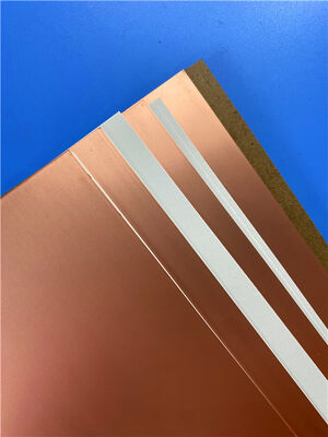
| Brand Name: | Wangling | Model Number: | F4BME275 |
|---|
Product Description
F4BME275 PTFE Laminate & Custom 2-Layer RF PCB – Complete Guide
What is F4BME275?
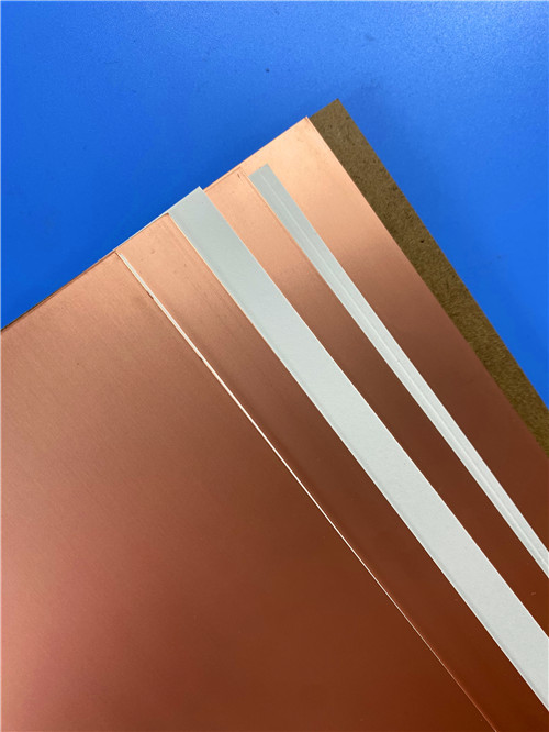
It is a high-performance PTFE glass fabric laminate. It has a dielectric constant (Dk) of 2.75 ±0.05. It has an ultra-low dissipation factor (Df) of 0.0015 at 10 GHz. It is manufactured by Taizhou Wangling Insulating Materials Factory in China. The material uses reverse-treated RTF copper foil. This provides superior low-PIM performance (≤ -159 dBc). It enables precise circuit etching. It also reduces conductor loss. The material can be used from -55°C to +260°C. It has a UL94 V-0 flammability rating. It is radiation-resistant and has low outgassing properties. It is an ideal replacement for imported PTFE laminates in demanding RF and microwave applications.
What PCB can be built with it?
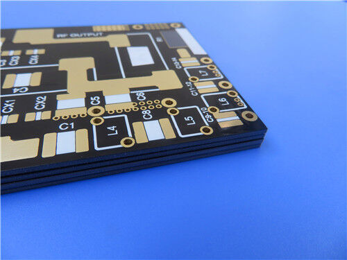
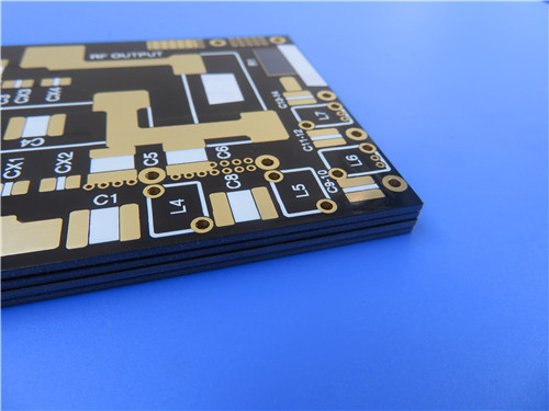
A complete 2-layer RF PCB solution can be provided. The board is based on F4BME275 material. The finished thickness is 1.6 mm. The copper weight is 1 oz per layer. Pure gold plating (5 µm) is applied. Black solder mask is applied on the top layer. White silkscreen is printed on the top layer. The minimum trace and space are 6 and 9 mils. The minimum hole size is 0.5 mm. Via plating thickness is 20 µm. The quality standard is IPC Class 2. This board is ideal for RF and microwave circuits, radar systems, satellite communications, and base station antennas.
1. Material Overview
The F4BME275 is a high-performance PTFE glass fabric laminate. It is produced by Taizhou Wangling Insulating Materials Factory. This factory is a leading Chinese supplier of RF and microwave substrates.
The material is made from woven fiberglass cloth, PTFE resin, and PTFE film. These components are combined through a scientific formulation. A rigorous compression molding process is used.
Important Points About This Material:
Better Performance: The F4BME series offers better electrical performance than the standard F4B series. The dielectric constant range is wider. Dielectric loss is lower. Insulation resistance is higher. Stability is improved.
RTF Copper Foil: F4BME275 uses reverse-treated RTF copper foil. This type of foil provides better PIM performance. PIM is reduced to ≤ -159 dBc. Circuit etching is more precise. Conductor loss is lower compared to standard ED copper.
Controlled Properties: The ratio of PTFE to fiberglass cloth is carefully adjusted. This allows the dielectric constant to be controlled. Low loss is maintained. Dimensional stability is improved.
Special Properties: The material is radiation-resistant. It has low outgassing properties. This makes it suitable for aerospace and satellite applications.
Commercial Production: The material is designed for high-volume production. It is cost-effective and commercially scalable.
F4BME275 vs. F4BM275 – Which One Should Be Chosen?
| Feature | F4BM275 | F4BME275 |
| Copper Foil Type | ED (Electrodeposited) | Reverse-treated RTF |
| PIM Performance | Not specified | ≤ -159 dBc |
| Circuit Precision | Standard | More precise |
| Conductor Loss | Standard | Lower |
| Best Application | General RF and microwave | Low-PIM systems, base stations, satellite |
Recommendation: F4BME275 should be chosen when PIM performance is critical. It should also be chosen when precision etching is needed. It is the better choice for base station antennas, satellite communications, and high-performance radar systems.
2. F4BME275 Technical Data Sheet
| Property | Test Condition | Unit | F4BME275 Value |
| Dielectric Constant (Typical) | 10 GHz | — | 2.75 |
| DK Tolerance | — | — | ±0.05 |
| Dissipation Factor (Typical) | 10 GHz | — | 0.0015 |
| 20 GHz | — | 0.0021 | |
| TCDk | -55°C ~ +150°C | ppm/°C | -92 |
| Peel Strength (1 oz ED / F4BM) | — | N/mm | >1.8 |
| (1 oz RTF / F4BME) | — | N/mm | >1.6 |
| Volume Resistivity | Normal condition | MΩ·cm | ≥6×10⁶ |
| Surface Resistivity | Normal condition | MΩ | ≥1×10⁶ |
| Electrical Strength (Z-direction) | 5 kW, 500 V/s | kV | >28 |
| Breakdown Voltage (X/Y-direction) | 5 kW, 500 V/s | kV | >35 |
| CTE (X/Y-axis) | -55°C ~ 288°C | ppm/°C | 14–16 |
| CTE (Z-axis) | -55°C ~ 288°C | ppm/°C | 112 |
| Thermal Stress | 260°C, 10s, 3 cycles | — | No delamination |
| Water Absorption | 20±2°C, 24 hrs | % | ≤0.08 |
| Density | Room temperature | g/cm³ | 2.28 |
| Continuous Operating Temperature | — | °C | -55 ~ +260 |
| Thermal Conductivity (Z-axis) | — | W/(m·K) | 0.38 |
| PIM Value (F4BME only) | — | dBc | ≤ -159 |
| Flammability | UL94 | Rating | V-0 |
| Composition | — | — | PTFE + Glass Fabric + RTF Copper |
3. Key Advantages of F4BME275
| Feature | Benefit |
| Dk is 2.75 ±0.05 | Tight tolerance allows consistent impedance control |
| Df is 0.0015 at 10 GHz | Ultra-low loss minimizes signal loss in high-frequency circuits |
| Df is 0.0021 at 20 GHz | Good performance is maintained at millimeter-wave frequencies |
| RTF copper foil is used | PIM is reduced (≤ -159 dBc), etching is more precise, conductor loss is lower |
| PIM is ≤ -159 dBc | This is critical for base station and satellite applications |
| Operating range is -55°C to +260°C | Extreme environments can be withstood |
| CTE (Z-axis) is 112 ppm/°C | Reliable plated through-hole performance is provided |
| Radiation resistance is provided | Aerospace and satellite-grade reliability is achieved |
| Low outgassing is ensured | This is important for vacuum environments |
| UL94 V-0 rating is achieved | Fire safety compliance is ensured |
4. Application Fields
-Microwave, RF, and Radar
-Phase Shifters, Passive Components
-Power Dividers, Couplers, Combiners
-Feed Networks, Phased Array Antennas
-Satellite Communication, Base Station Antennas
5. Custom 2-Layer RF PCB – Complete Specification
A complete 2-layer RF PCB solution can be provided based on F4BME275. The specifications are shown below.
Board Specifications
| Specification | Detail |
| Board Type | 2-Layer RF PCB |
| Base Material | F4BME275 PTFE Laminate (RTF Copper) |
| Finished Board Thickness | 1.6 mm |
| Finished Copper Weight | 1 oz (35 µm) per layer |
| Board Dimensions | 103 × 76 mm (1 piece) |
| Dimension Tolerance | ±0.15 mm |
| Minimum Trace / Space | 6 / 9 mils |
| Minimum Hole Size | 0.5 mm |
| Via Plating Thickness | 20 µm |
| Surface Finish | Pure Gold Plating (5 µm / 197 µ") |
| Top Solder Mask | Black |
| Bottom Solder Mask | No |
| Top Silkscreen | White |
| Bottom Silkscreen | No |
| IPC Classification | Class 2 |
| Artwork Format | Gerber RS-274-X |
| Testing | 100% Electrical Test (before shipment) |
| Availability | Worldwide |
6. Why Pure Gold Finish Is Used
Pure gold plating (5 µm / 197 µ") is chosen for this RF PCB. The advantages are listed below.
| Advantage | Benefit |
| Excellent solderability is provided | An oxidation-free surface is available for component attachment |
| Wire bonding is supported | RF components that require gold wire bonding can be used |
| Corrosion resistance is provided | Copper traces are protected in harsh environments |
| Low contact resistance is achieved | This is suitable for edge connectors and test points |
| Long shelf life is maintained | Solderability is preserved over extended periods |
| Thicker gold (5 µm) is applied | Extra durability is provided for high-reliability applications |
Q1: What is the difference between F4BME275 and F4BM275?
A: The same PTFE/glass dielectric is used (Dk 2.75). However, the copper foil type is different.
F4BME275 uses reverse-treated RTF copper foil. PIM performance is superior (≤ -159 dBc). Etching is more precise. Conductor loss is lower.
F4BM275 uses standard ED copper foil. It is suitable for general RF applications. PIM requirements are not met.
F4BME275 should be chosen for base stations, satellite systems, and low-PIM-sensitive applications.
Q2: What is PIM and why is it important?
A: PIM stands for Passive Intermodulation. It is distortion that is generated when high-power signals pass through nonlinear elements in passive components. Low-PIM performance (≤ -159 dBc for F4BME275) is important for:
Base station antennas (cell towers)
Satellite communications
Radar systems
High-power RF systems
High PIM can cause interference. Receiver sensitivity is reduced. System performance is degraded.
Q3: Why is pure gold plating used instead of ENIG?
A: Pure gold plating (5 µm / 197 µ") offers several advantages over standard ENIG:
Thicker gold is applied — better wear resistance and longer shelf life are provided
Wire bonding is supported — ENIG is generally not suitable for wire bonding
Superior corrosion resistance is provided — this is important for harsh environments
Lower contact resistance is achieved — this is better for edge connectors and test points
ENIG is typically used for SMT assembly. Pure gold is preferred for RF components that require wire bonding or high durability.
Q4: What does 6/9 mil trace and space mean?
A: 6 mil trace — The minimum conductor width is 6 mils (0.152 mm).
9 mil space — The minimum spacing between conductors is 9 mils (0.229 mm).
This fine-line capability enables high-density RF circuit layouts. Controlled impedance transmission lines can be produced.
Q5: Why is there no solder mask on the bottom layer?
A: This design provides several benefits:
Thermal management is improved — exposed copper aids in heat dissipation
Grounding is enabled — direct chassis grounding or thermal pad contact is possible
Component placement is simplified — the bottom side has no SMT components (all SMT pads are on top)
This is a common design practice for RF PCBs. Thermal performance and grounding are often priorities.
Q6: Is F4BME275 suitable for lead-free soldering?
A: Yes. The continuous operating temperature range is -55°C to +260°C. Thermal stress testing at 260°C for 10 seconds (3 cycles) shows no delamination. F4BME275 is fully compatible with lead-free soldering processes.
Q7: What is the typical lead time for custom F4BME275 PCBs?
A: Lead times vary based on complexity and quantity. For 2-layer RF PCBs like the example described, typical lead times are 7 to 12 working days. Please contact us for specific project timelines.
Q8: Are aluminum-backed or copper-backed versions of F4BME275 available?
A: Yes. F4BME275 is available in aluminum-backed (F4BME275-AL) and copper-backed (F4BME275-CU) versions. These are used for enhanced thermal management and shielding. They are ideal for high-power RF applications.
Q9: Can impedance-controlled PCBs be produced with F4BME275?
A: Yes. The stable Dk of 2.75 ±0.05 allows predictable impedance control. Impedance-controlled RF boards can be designed and manufactured to your specific requirements.
Q10: What testing is performed on these PCBs?
A: All boards undergo:
100% electrical test (before shipment) — continuity and isolation are verified
Visual inspection — solder mask and silkscreen quality are checked
Dimensional inspection — board dimensions and tolerances (±0.15 mm) are confirmed
Additional testing (e.g., impedance testing, X-ray for BGA) can be arranged upon request.
Q11: What is the minimum dielectric thickness for F4BME275?
A: For Dk 2.7–3.0 (including F4BME275 at Dk 2.75), the minimum dielectric thickness is 0.2 mm. For Dk ≤2.65, the minimum dielectric thickness is 0.1 mm.
Q12: Where can the official F4BME275 data sheet be obtained?
A: The official data sheet is available from Taizhou Wangling Insulating Materials Factory. Please contact our team. We can provide the documentation. We can also direct you to the manufacturer's technical support.
Ready to Get Started?
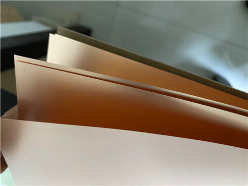
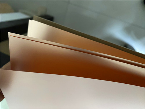
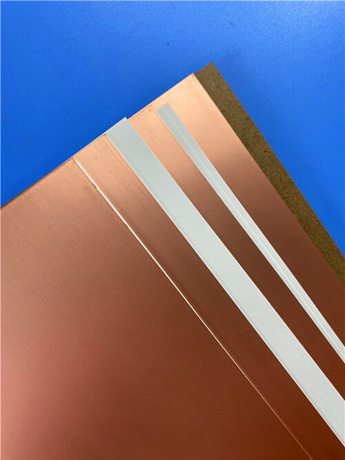
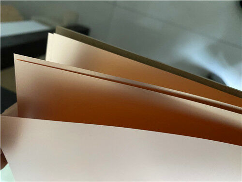
Raw F4BME275 laminate can be provided. Metal-backed variants are also available. Fully fabricated 2-layer RF PCBs with pure gold finish and fine-line capability can be manufactured.
Contact us today for:
Material sampling and testing
RF circuit design assistance
Impedance calculation and design support
PCB quoting and DFM review
Technical support for your specific application
Enter Your Message

RO4350B, 4003C; Rogers 5880, 5870, 6002, 6010, 6006, 6035; RO3003, RO3035, RO3006, RO3010, RO3210,RO3203
TLX-8, TLX-6, TLX-9, TLX-0, TLX-7, TLY-3, TLY-5, RF-35TC, RF-60TC, RF-35A2, RF-60A, AD450, AD600, TMM4, TC350
| Shenzhen Bicheng Electronics Technology Co., Ltd |
| 6-11C Shidai Jingyuan Fuyong Town, Baoan District, Shenzhen City, Guangdong Province, China |
| 86-755-27374946 |
| sales30@bichengpcb.com |