



F4BME275 PTFE Laminate : Dk 2.75, Df 0.0015, PIM ≤ -159 dBc – Is It Right for Your RF PCB?
Contact Person : Sally Mao
Phone Number : 86-755-27374847
WhatsApp : +8618277967574
| Supply Ability : | 50000pcs |
|---|
| Brand Name: | Wangling | Model Number: | F4BTD350S |
|---|
Product Description
What is F4BTD350S?
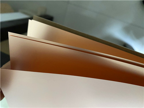
It is a high-thermal-conductivity PTFE resin high-frequency substrate. It is reinforced with glass fiber cloth. It contains a large amount of high-thermal-conductivity special ceramics. The dielectric constant (Dk) is 3.5 ±0.07 at 10 GHz. The dissipation factor (Df) is 0.0016 at 10 GHz. The thermal conductivity is 1.25 W/(m·K). This is significantly higher than standard PTFE materials. The material has a CTE of 11/10 ppm/°C in the X/Y axes and 40 ppm/°C in the Z axis. The decomposition temperature (Td) is 500°C. The material is UL94 V-0 rated. It has very low moisture absorption (0.05%). It is ideal for high-power RF applications that require low insertion loss and efficient heat dissipation.
What PCB can be built with it?
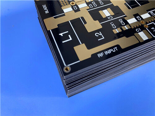
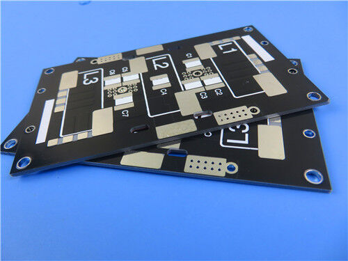
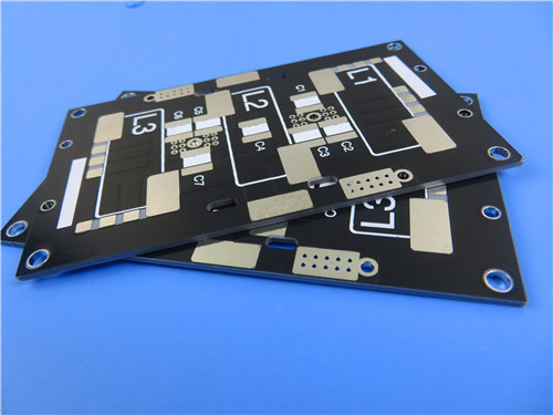
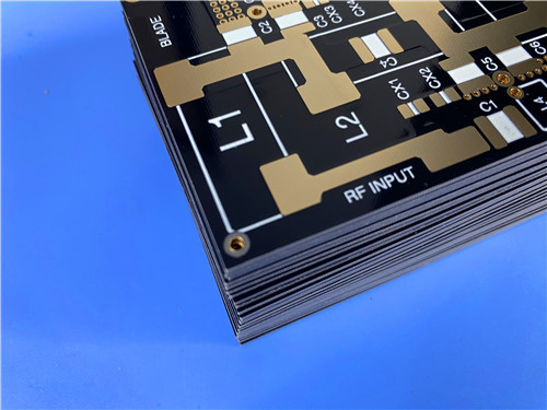
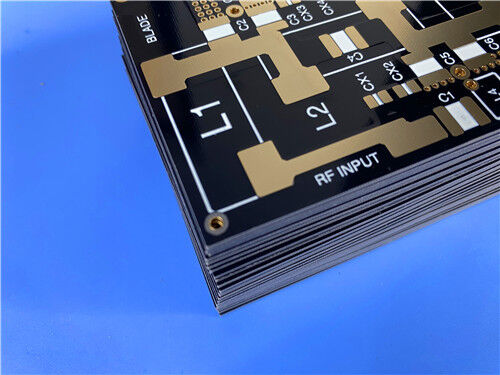
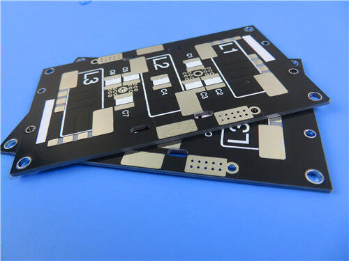
A complete 2-layer RF PCB solution can be provided. The board is based on F4BTD350S material. The finished thickness is 0.6 mm. The copper weight is 1 oz per layer. Immersion gold is applied as the surface finish. Black solder mask is applied on the top layer. White silkscreen is printed on the top layer. No solder mask or silkscreen is applied on the bottom layer. The minimum trace and space are 7 and 9 mils. The minimum hole size is 0.6 mm. Via plating thickness is 20 µm. The quality standard is IPC Class 2. This board is ideal for high-power RF amplifiers, antennas, couplers, filters, and industrial heating equipment.
1. Material Overview
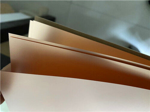
The F4BTD350S is a high-thermal-conductivity PTFE resin high-frequency substrate. It is manufactured by Taizhou Wangling Insulating Materials Factory. It is reinforced with glass fiber cloth. It contains a large amount of high-thermal-conductivity special ceramics.
This material is a new generation of high-frequency materials. It was developed for applications that require low insertion loss and high heat dissipation efficiency. It can replace similar foreign products.
The excellent low loss and thermal conductivity performance increase the microwave power tolerance. The service life of devices is extended. The material is more suitable for high-temperature and long-term operation. Equipment reliability is ensured. Low-cost maintenance is achieved.
The material also has the following advantages:
Low thermal expansion coefficient
Dimensional stability
High electrical strength
High insulation performance
These advantages make PCB processing easier. Through-hole reliability is higher. Soldering faults are lower. Component matching is better. Environmental adaptability is stronger.
The circuit boards can be processed using standard PTFE sheet technology. The excellent mechanical and physical properties make the material suitable for multilayer, high-multilayer, and backplane processing. It also shows excellent processability in dense hole and fine-line processing.
2. F4BTD350S Technical Data Sheet
| Property | Test Condition | Unit | F4BTD350S Value |
| Dielectric Constant (Typical) | 2 GHz | — | 3.52 |
| 10 GHz | — | 3.5 | |
| DK Tolerance | — | — | ±0.07 |
| Dielectric Constant (Design) | 10 GHz | — | 3.62 |
| Loss Factor (Typical) | 2 GHz | — | 0.0012 |
| 10 GHz | — | 0.0016 | |
| TCDk | -55°C to 150°C | ppm/°C | -45 |
| Peel Strength (1 oz copper foil) | — | N/mm | >0.8 |
| Volume Resistivity | C96/23/95 | MΩ·cm | 1×10¹¹ |
| Surface Resistance | C96/23/95 | MΩ | 1×10¹² |
| Electric Strength (Z-direction) | 5 kW, 500 V/s | kV/mm | 25 |
| Breakdown Voltage (Horizontal) | 5 kW, 500 V/s | kV | 38 |
| Relative Tracking Index (CTI) | 23°C/50%/24H | V | 600 |
| CTE (X-axis) | -55°C to 288°C | ppm/°C | 11 |
| CTE (Y-axis) | -55°C to 288°C | ppm/°C | 10 |
| CTE (Z-axis) | -55°C to 288°C | ppm/°C | 40 |
| Thermal Decomposition Temp (Td) | 5% mass loss | °C | 500 |
| Flexural Strength (X/Y) | Normal state | MPa | 74/64 |
| Tensile Strength (X/Y) | Normal state | MPa | 48/45 |
| Flexural Modulus (X/Y) | Normal state | MPa | 7500/7000 |
| Dimensional Stability (X/Y) | After etching and baking | % | 0.08/0.18 |
| Thermal Stress | 260°C/10s/3 times | — | No delamination |
| Thermal Conductivity | Z-direction | W/(m·K) | 1.25 |
| Specific Heat Capacity | — | J/g·°C | 0.8 |
| Density | Normal temperature | g/cm³ | 2.21 |
| Long-term Service Temperature | — | °C | -55 to +260 |
| Water Absorption | 20±2°C, 24 hours | % | 0.05 |
| Flame Retardancy | UL94 | Rating | V-0 |
| Dielectric Layer Composition | — | — | PTFE + Glass Fiber Cloth + High-Thermal-Conductivity Ceramics |
3. Application Fields
- High power radio frequency
- Power amplifier
- Antenna
- Industrial heating equipment
- Couplers, filters, power splitters
4. Custom 2-Layer RF PCB – Complete Specification
A complete 2-layer RF PCB solution can be provided based on F4BTD350S.
Board Specifications
| Specification | Detail |
| Board Type | 2-Layer RF PCB |
| Base Material | F4BTD350S (0.508 mm / 20 mil core) |
| Finished Board Thickness | 0.6 mm |
| Finished Copper Weight | 1 oz (35 µm) per layer |
| Board Dimensions | 79 × 110 mm (1 piece) |
| Dimension Tolerance | ±0.15 mm |
| Minimum Trace / Space | 7 / 9 mils |
| Minimum Hole Size | 0.6 mm |
| Via Plating Thickness | 20 µm |
| Surface Finish | Immersion Gold (ENIG) |
| Top Solder Mask | Black |
| Bottom Solder Mask | No |
| Top Silkscreen | White |
| Bottom Silkscreen | No |
| IPC Classification | Class 2 |
| Artwork Format | Gerber RS-274-X |
| Testing | 100% Electrical Test (before shipment) |
| Availability | Worldwide |
5. Key Benefits of This PCB Design
| Feature | Benefit |
| 2-layer RF design is used | Simple and cost-effective RF circuit implementation is achieved |
| F4BTD350S core (0.508 mm) is used | High thermal conductivity (1.25 W/m·K) dissipates heat efficiently; low loss (0.0016) ensures signal integrity |
| 7/9 mil trace and space are used | Fine-line, high-density RF circuits can be produced |
| Black solder mask is applied on top | Professional appearance; top-layer circuits are protected |
| No solder mask on bottom | Thermal dissipation is improved; grounding strategies are enabled |
| Immersion gold finish is applied | Excellent solderability; oxidation resistance; flat surface |
| 20 µm via plating is used | Reliable plated through-hole connections are ensured |
| IPC Class 2 quality is met | Commercial and industrial quality standards are satisfied |
| 100% electrical test is performed | Functional integrity is guaranteed before shipment |
Q1: What is the dielectric constant of F4BTD350S?
The typical Dk is 3.5 ±0.07 at 10 GHz. The design Dk is 3.62 at 10 GHz. The Dk is stable over temperature with a TCDk of -45 ppm/°C.
Q2: What is the thermal conductivity of F4BTD350S?
The thermal conductivity is 1.25 W/(m·K) in the Z-direction. This is significantly higher than standard PTFE materials. It allows efficient heat dissipation in high-power RF applications.
Q3: Is F4BTD350S suitable for high-power RF applications?
Yes. The material was specifically developed for high-power RF applications. The high thermal conductivity (1.25 W/(m·K)) dissipates heat efficiently. The low loss (0.0016) minimizes signal attenuation. The high power tolerance allows high microwave power levels to be handled.
Q4: What thicknesses are available for F4BTD350S?
Dielectric thicknesses are available from 0.127 mm (5 mil) to 6.35 mm (250 mil). Standard sizes include 305×460 mm and 460×610 mm. Copper foil thicknesses of 0.5 oz and 1 oz are standard. Other thicknesses can be customized.
Q5: Where can the official F4BTD350S data sheet be obtained?
The official data sheet is available from Taizhou Wangling Insulating Materials Factory. Please contact our team. We can provide the documentation. We can also direct you to the manufacturer's technical support.
Ready to Get Started?
F4BTD350S raw laminate can be provided. Metal-backed variants (aluminum or copper) are also available. Fully fabricated 2-layer RF PCBs with immersion gold finish can be manufactured.
Contact us today for:
Material sampling and testing
RF circuit design assistance
Impedance calculation and design support
PCB quoting and DFM review
Technical support for your specific application
Enter Your Message

RO4350B, 4003C; Rogers 5880, 5870, 6002, 6010, 6006, 6035; RO3003, RO3035, RO3006, RO3010, RO3210,RO3203
TLX-8, TLX-6, TLX-9, TLX-0, TLX-7, TLY-3, TLY-5, RF-35TC, RF-60TC, RF-35A2, RF-60A, AD450, AD600, TMM4, TC350
| Shenzhen Bicheng Electronics Technology Co., Ltd |
| 6-11C Shidai Jingyuan Fuyong Town, Baoan District, Shenzhen City, Guangdong Province, China |
| 86-755-27374946 |
| sales30@bichengpcb.com |