Product Description
What is WL-CT350?
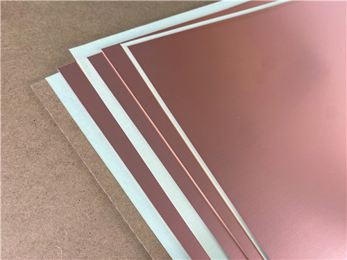
It is a thermosetting resin-based high-frequency laminate manufactured by Taizhou Wangling Insulating Materials Factory. It is part of the WL-CT series. The dielectric layer is composed of hydrocarbon resin, ceramics, and fiberglass cloth. The dielectric constant (Dk) is 3.48 at 10 GHz. The dissipation factor (Df) is 0.0039 at 10 GHz. The material has a Tg greater than 280°C. The thermal conductivity is 0.70 W/(m·K). The CTE in the X and Y axes is 11 and 14 ppm/°C. The Z-axis CTE is 34 ppm/°C. The material can be processed using standard FR-4 techniques. This is simpler than PTFE processing. The material offers better stability and consistency in circuitry.
What PCB can be built with it?
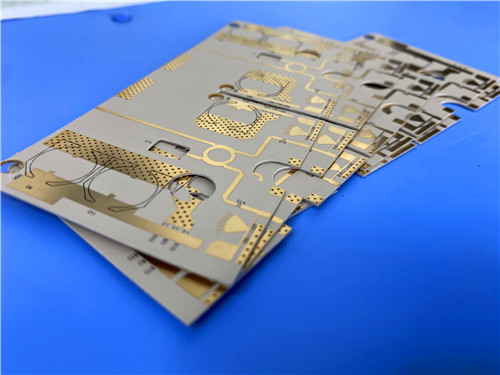
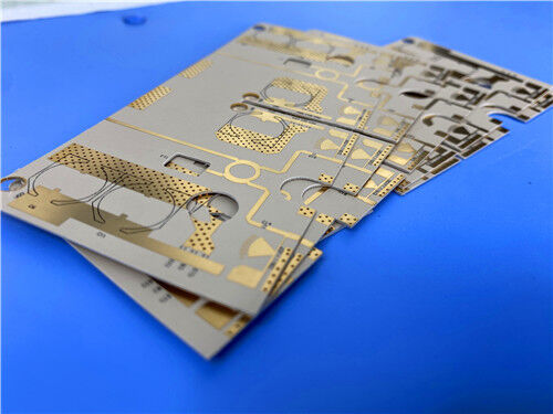
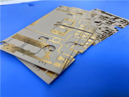
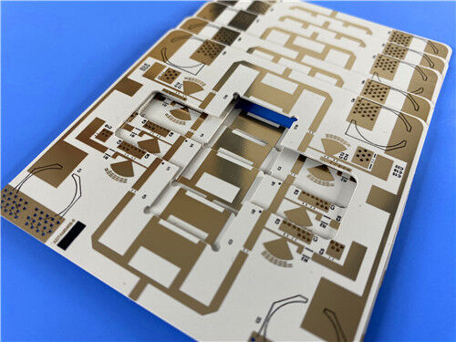
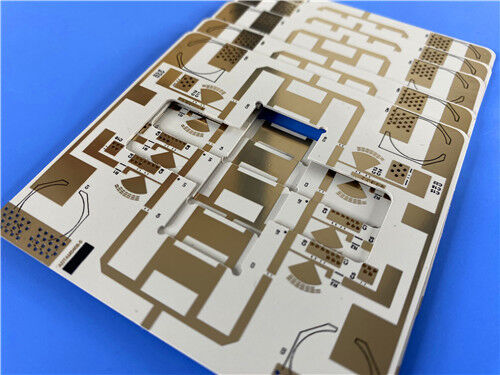
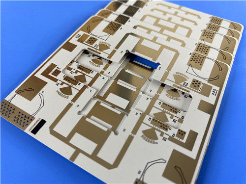
A complete 2-layer RF PCB solution can be provided. The board is based on WL-CT350 material. The finished thickness is 0.2 mm. The copper weight is 1 oz per layer. Immersion gold is applied as the surface finish. No solder mask is applied on either side. Black silkscreen is printed on the top layer. The minimum trace and space are 6 and 7 mils. The minimum hole size is 0.3 mm. Via plating thickness is 20 µm. The quality standard is IPC Class 2. This board is ideal for base station antennas, satellite antennas, automotive radar, power amplifiers, RF devices, and filters.

Material Overview
The WL-CT350 is a thermosetting resin-based high-frequency laminate. It is manufactured by Taizhou Wangling Insulating Materials Factory. It is part of the WL-CT series. The dielectric layer is composed of hydrocarbon resin, ceramics, and fiberglass cloth.
The material offers low loss performance. It meets the requirements for high-frequency designs. PCB processing can be carried out using techniques similar to FR-4 materials. This is simpler compared to PTFE materials. Better stability and consistency in circuitry are ensured. The material can be used as a substitute for similar foreign products.
The combination of hydrocarbon resin and composite ceramics provides several advantages:
Excellent low loss
High-temperature resistance
Temperature stability
Low thermal expansion coefficient
High Tg greater than 280°C
Why Choose WL-CT350 Over PTFE:
| Feature |
WL-CT350 (Thermoset) |
PTFE-Based Materials |
| Processing |
Standard FR-4 techniques |
Specialized PTFE techniques |
| Via Preparation |
No sodium etch required |
Sodium etch often required |
| Panel Handling |
Rigid, automated handling |
Soft, specialized handling |
| Dimensional Stability |
Excellent |
Good (with glass reinforcement) |
| Tg |
>280°C |
N/A (PTFE softens) |
| Wire Bonding |
Reliable (thermoset) |
Risk of pad lifting |
| Cost |
Cost-effective |
More expensive |
WL-CT350 Technical Data Sheet
| Property |
Test Condition |
Unit |
WL-CT350 Value |
| Dielectric Constant (Typical) |
10 GHz |
— |
3.48 |
| Dielectric Constant (Design) |
10 GHz |
— |
3.66 |
| DK Tolerance |
— |
— |
±0.05 |
| Dissipation Factor (Typical) |
2 GHz |
— |
0.003 |
| |
10 GHz |
— |
0.0039 |
| |
20 GHz |
— |
0.0048 |
| TCDk |
-55°C to 150°C |
ppm/°C |
52 |
| Peel Strength (1 oz ED) |
— |
N/mm |
0.85 |
| (1 oz RTF) |
— |
N/mm |
0.72 |
| Volume Resistivity |
Normal condition |
MΩ·cm |
1×10⁹ |
| Surface Resistivity |
Normal condition |
MΩ |
4×10⁹ |
| Electrical Strength (Z-direction) |
5 kW, 500 V/s |
kV/mm |
31 |
| Breakdown Voltage (X/Y-direction) |
5 kW, 500 V/s |
kV |
30 |
| CTE X-axis |
-55°C to 288°C |
ppm/°C |
11 |
| CTE Y-axis |
-55°C to 288°C |
ppm/°C |
14 |
| CTE Z-axis |
-55°C to 288°C |
ppm/°C |
34 |
| Thermal Stress |
288°C, 10s, 3 times |
— |
No delamination |
| Water Absorption |
23.5±2°C, 24 hours |
% |
0.05 |
| Density |
Normal temperature |
g/cm³ |
1.9 |
| Long-term Service Temperature |
— |
°C |
-55 to +260 |
| Thermal Conductivity |
Z-direction |
W/(m·K) |
0.7 |
| PIM Value (with RTF copper) |
— |
dBc |
≤ -157 |
| Flammability |
UL94 |
Rating |
V-0 |
| Tg |
— |
°C |
>280 |
| Td |
Onset |
°C |
386 |
| Halogen Content |
— |
— |
Halogenated |
| Composition |
— |
— |
Hydrocarbon + Ceramic + Glass Fabric |
Key Advantages of WL-CT350
| Feature |
Benefit |
| Dk is 3.48 ±0.05 |
Tight tolerance allows consistent impedance control |
| Df is 0.0039 at 10 GHz |
Low loss minimizes signal attenuation in microwave circuits |
| Tg is >280°C |
Withstands lead-free soldering without deformation |
| Td is 386°C |
Good thermal decomposition resistance |
| TCDk is 52 ppm/°C |
Stable Dk over temperature ensures consistent performance |
| CTE X/Y is 11/14 ppm/°C |
CTE matches copper; excellent dimensional stability |
| CTE Z is 34 ppm/°C |
Good plated through-hole reliability is ensured |
| Thermal conductivity is 0.70 W/(m·K) |
Heat dissipation is improved for power applications |
| Moisture absorption is 0.05% |
Very low water absorption ensures stable performance |
| UL94 V-0 rating is achieved |
Fire safety compliance is ensured |
| FR-4 processability |
No specialized equipment required; lower fabrication cost |
| Thermoset resin is used |
No softening when heated; reliable wire bonding |
| Radiation resistance is provided |
Suitable for aerospace applications |
| Low outgassing is ensured |
Suitable for space applications |
WL-CT350 vs. WL-CT Series Variants
The WL-CT series offers multiple dielectric constants. The options are listed below.
| Material |
Dk at 10 GHz |
Best Application |
| WL-CT300 |
3 |
General RF |
| WL-CT330 |
3.3 |
RF and microwave |
| WL-CT338 |
3.38 |
High-frequency RF |
| WL-CT348 |
3.48 |
RF, antennas, automotive radar |
| WL-CT410 |
4.1 |
Higher Dk requirements |
| WL-CT615 |
6.15 |
High-DK applications |
Application Fields
- Base station antennas and satellite antennas.
- Automotive radar, sensors, and navigation systems.
- Power amplifiers.
- Satellite high-frequency heads.
- RF devices and filters.
- WIMAX antennas and distributed antennas.
Custom 2-Layer RF PCB – Complete Specification
A complete 2-layer RF PCB solution can be provided based on WL-CT350. The specifications are shown below.
Board Specifications
| Specification |
Detail |
| Board Type |
2-Layer RF PCB |
| Base Material |
WL-CT350 (0.102 mm / 4 mil core) |
| Finished Board Thickness |
0.2 mm |
| Finished Copper Weight |
1 oz (35 µm) per layer |
| Board Dimensions |
56.8 × 78.09 mm (1 piece) |
| Dimension Tolerance |
±0.15 mm |
| Minimum Trace / Space |
6 / 7 mils |
| Minimum Hole Size |
0.3 mm |
| Via Plating Thickness |
20 µm |
| Surface Finish |
Immersion Gold (ENIG) |
| Top Solder Mask |
No |
| Bottom Solder Mask |
No |
| Top Silkscreen |
Black |
| Bottom Silkscreen |
No |
| IPC Classification |
Class 2 |
| Artwork Format |
Gerber RS-274-X |
| Testing |
100% Electrical Test (before shipment) |
| Availability |
Worldwide |
Key Benefits of This PCB Design
| Feature |
Benefit |
| 2-layer RF design is used |
Simple and cost-effective RF circuit implementation is achieved |
| WL-CT350 core (0.102 mm) is used |
Low loss (0.0039), stable Dk (3.48), and FR-4 processability |
| Thin 0.2 mm board |
Ultra-lightweight and compact design is achieved |
| 6/7 mil trace and space are used |
Fine-line, high-density RF circuits can be produced |
| No solder mask is used on either side |
Weight and cost are reduced; RF performance is optimized |
| Immersion gold finish is applied |
Excellent solderability; oxidation resistance; flat surface |
| 20 µm via plating is used |
Reliable plated through-hole connections are ensured |
| IPC Class 2 quality is met |
Commercial and industrial quality standards are satisfied |
| 100% electrical test is performed |
Functional integrity is guaranteed before shipment |
Q1: What is the dielectric constant of WL-CT350?
The typical Dk is 3.48 at 10 GHz and 23°C. The design Dk is 3.66 at 10 GHz. The Dk tolerance is ±0.05.
Q2: How does WL-CT350 compare to PTFE materials?
WL-CT350 is a thermosetting hydrocarbon material. It offers similar high-frequency performance to PTFE. However, it can be processed using standard FR-4 techniques. No specialized equipment is required. This reduces fabrication cost and lead time. It also offers better dimensional stability and reliability.
Q3: What is the maximum operating temperature of WL-CT350?
The long-term service temperature is -55°C to +260°C. The Tg is greater than 280°C. This ensures stable performance during lead-free soldering. It also ensures reliability in high-temperature environments.
Q4: What copper foil options are available for WL-CT350?
Two copper foil options are available:
ED copper – suitable for general applications
RTF copper – offers better PIM performance (≤ -157 dBc), lower conductor loss, and more precise etching
RTF copper adds approximately 0.018 mm (0.7 mil) to the dielectric thickness.
Ready to Get Started?
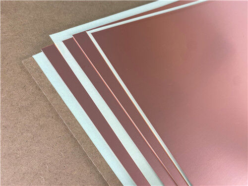
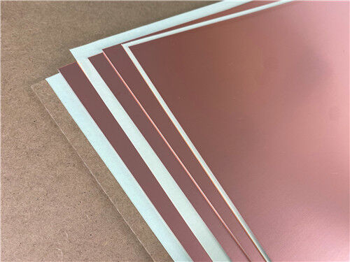
WL-CT350 raw laminate can be provided. Aluminum-backed variants are also available. Fully fabricated 2-layer RF PCBs with immersion gold finish can be manufactured.
Contact us today for:
Material sampling and testing
RF circuit design assistance
Impedance calculation and design support
PCB quoting and DFM review
Technical support for your specific application


 Your message must be between 20-3,000 characters!