


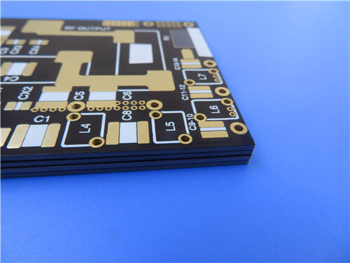
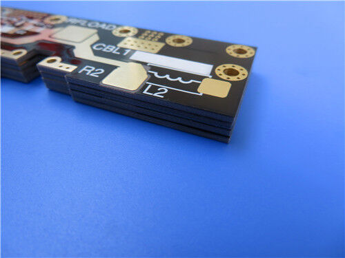
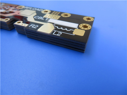
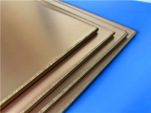
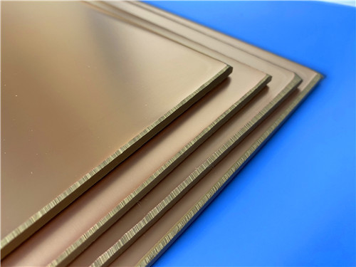

F4BTME350 Ceramic-Filled PTFE Laminate with Reverse-Treated Copper and Custom 2-layer PCB built on 10mil substrate material for RF Microwave
Contact Person : Sally Mao
Phone Number : 86-755-27374847
WhatsApp : +8618277967574
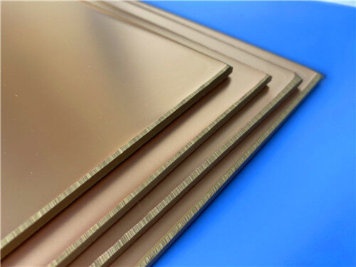
| Brand Name: | Wangling | Model Number: | F4BTM300 |
|---|
Product Description
In the pursuit of higher dielectric constants without sacrificing low-loss performance, ceramic-filled PTFE laminates have become a cornerstone of modern RF and microwave design. The F4BTM300 from Taizhou Wangling Insulation Materials Factory represents a compelling option for engineers seeking a balance of high dielectric constant, thermal stability, and cost-effective manufacturability.
F4BTM300 is a glass fiber cloth reinforced, nano-ceramic-filled PTFE laminate. By incorporating high-dielectric, low-loss nano-ceramics into the F4BM dielectric layer, the material achieves a higher dielectric constant, improved heat resistance, lower thermal expansion, higher insulation resistance, and better thermal conductivity—all while preserving its low-loss character.
The F4BTM series is available with ED copper foil (suitable for applications without strict PIM requirements), while the F4BTME variant pairs the same dielectric with reverse-treated RTF copper foil for excellent PIM performance, precise line control, and reduced conductor loss.
Key Properties at a Glance (F4BTM300):
| Product Technical Parameters | Product Models & Data Sheet | ||||||
| Product Features | Test Conditions | Unit | F4BTM298 | F4BTM300 | F4BTM320 | F4BTM350 | |
| Dielectric Constant (Typical) | 10GHz | / | 2.98 | 3.0 | 3.2 | 3.5 | |
| Dielectric Constant Tolerance | / | / | ±0.06 | ±0.06 | ±0.06 | ±0.07 | |
| Loss Tangent (Typical) | 10GHz | / | 0.0018 | 0.0018 | 0.0020 | 0.0025 | |
| 20GHz | / | 0.0023 | 0.0023 | 0.0026 | 0.0035 | ||
| Dielectric Constant Temperature Coefficient | -55 º~150ºC | PPM/℃ | -78 | -75 | -75 | -60 | |
| Peel Strength | 1 OZ F4BTM | N/mm | >1.6 | >1.6 | >1.6 | >1.6 | |
| 1 OZ F4BTME | N/mm | >1.4 | >1.4 | >1.4 | >1.4 | ||
| Volume Resistivity | Standard Condition | MΩ.cm | ≥1×10^7 | ≥1×10^7 | ≥1×10^7 | ≥1×10^7 | |
| Surface Resistivity | Standard Condition | MΩ | ≥1×10^6 | ≥1×10^6 | ≥1×10^6 | ≥1×10^6 | |
| Electrical Strength (Z direction) | 5KW,500V/s | KV/mm | >26 | >30 | >32 | >32 | |
| Breakdown Voltage (XY direction) | 5KW,500V/s | KV | >34 | >35 | >40 | >40 | |
| Coefficientof Thermal Expansion | XY direction | -55 º~288ºC | ppm/ºC | 15,16 | 15,16 | 13,15 | 10,12 |
| Z direction | -55 º~288ºC | ppm/ºC | 78 | 72 | 58 | 51 | |
| Thermal Stress | 260℃, 10s,3 times | No delamination | No delamination | No delamination | No delamination | ||
| Water Absorption | 20±2℃, 24 hours | % | ≤0.05 | ≤0.05 | ≤0.05 | ≤0.05 | |
| Density | Room Temperature | g/cm3 | 2.25 | 2.25 | 2.20 | 2.20 | |
| Long-Term Operating Temperature | High-Low Temperature Chamber | ℃ | -55~+260 | -55~+260 | -55~+260 | -55~+260 | |
| Thermal Conductivity | Z direction | W/(M.K) | 0.42 | 0.42 | 0.50 | 0.54 | |
| PIM | Only applicable to F4BTME | dBc | ≤-160 | ≤-160 | ≤-160 | ≤-160 | |
| Flammability | / | UL-94 | V-0 | V-0 | V-0 | V-0 | |
| Material Composition | / | / | PTFE, Fiberglass Cloth, nano-ceramics F4BTM paired with ED copper foil, F4BTME paired with reverse-treated (RTF) copper foil. |
||||
Our PCB Capability (F4BTM)
| PCB Capability (F4BTM) | |||
| PCB Material: | PTFE / glass fiber cloth / Nano-ceramic filler | ||
| Designation (F4BTM ) | F4BTM | DK (10GHz) | DF (10 GHz) |
| F4BTM298 | 2.98±0.06 | 0.0018 | |
| F4BTM300 | 3.0±0.06 | 0.0018 | |
| F4BTM320 | 3.2±0.06 | 0.0020 | |
| F4BTM350 | 3.5±0.07 | 0.0025 | |
| Layer count: | Single Sided, Double Sided PCB, Multilayer PCB, Hybrid PCB | ||
| Copper weight: | 0.5oz (17 µm), 1oz (35µm), 2oz (70µm) | ||
| Dielectric thickness (or overall thickness) | 0.25mm, 0.508mm, 0.762mm, 0.8mm, 1.0mm, 1.016mm, 1.27mm, 1.524mm, 2.0mm, 3.0mm, 4.0mm, 5.0mm, 6.0mm, 8.0mm, 10.0mm, 12.0mm | ||
| PCB size: | ≤400mm X 500mm | ||
| Solder mask: | Green, Black, Blue, Yellow, Red etc. | ||
| Surface finish: | Bare copper, HASL, ENIG, Immersion silver, Immersion tin, OSP, Pure gold, ENEPIG etc.. |
||
Applications
The F4BTM300 laminate is engineered for demanding RF and microwave environments, with typical applications including:
Custom PCB Manufacturing on F4BTM300
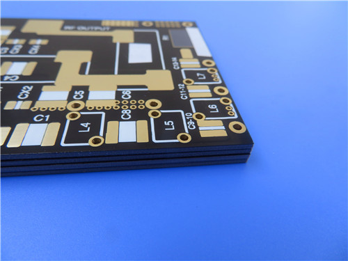
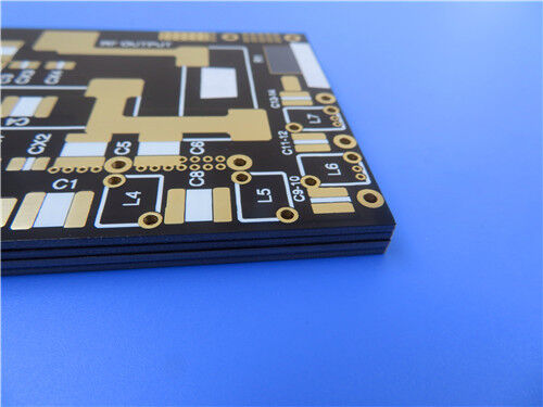
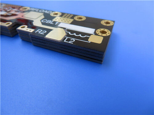
As a specialized manufacturer of high-frequency printed circuit boards, we offer comprehensive fabrication services using F4BTM300 and other advanced materials. The following specification details a representative 2-layer rigid PCB implementation:
PCB Construction Details:
| Parameter | Specification |
| Base Material | F4BTM300 |
| Layer Count | 2-layer rigid |
| Board Dimensions | 105.4mm × 76mm per panel, ±0.15mm |
| Finished Thickness | 0.6mm |
| Copper Weight | 1 oz (1.4 mils) outer layers |
| Minimum Trace/Space | 5 / 8 mils |
| Minimum Hole Size | 0.35mm |
| Via Structure | No blind or buried vias |
| Via Plating Thickness | 20 μm |
| Surface Finish | Immersion Gold |
| Solder Mask | Black, top side only |
| Silkscreen | White, top side only |
| Electrical Test | 100% prior to shipment |
| Artwork Format | Gerber RS-274-X |
| Quality Standard | IPC-Class-2 |
PCB Statistics:
| Metric | Count |
| Components | 13 |
| Total Pads | 94 |
| Through-Hole Pads | 51 |
| Top SMT Pads | 43 |
| Bottom SMT Pads | 0 |
| Vias | 36 |
| Nets | 2 |
Material Advantages
Higher Dielectric Constant with Low Loss:
The addition of nano-ceramics raises the Dk to 3.0 while maintaining a low dissipation factor of 0.0018 at 10 GHz and 0.0023 at 20 GHz. This enables more compact circuit designs without sacrificing signal integrity.
Excellent Thermal Stability:
With a CTE of 15 ppm/°C in X and 16 ppm/°C in Y (matched to copper), plus a low dielectric constant temperature coefficient of -75 ppm/°C, F4BTM300 maintains stable electrical performance across temperature extremes from -55°C to +260°C.
Superior PIM Performance (F4BTME):
When paired with reverse-treated RTF copper foil, the F4BTME variant achieves PIM values of ≤ -160 dBc, making it an excellent choice for sensitive receive paths in base station and satellite antennas.
Improved Thermal Management:
A thermal conductivity of 0.42 W/m·K in the Z-direction helps dissipate heat in high-power RF applications, while the material's high insulation resistance and breakdown voltage (>35 kV in XY direction) ensure reliable operation.
Cost-Effective and Scalable:
As a commercially available, mass-producible material, F4BTM300 offers a high cost-performance ratio with a wide range of available thicknesses (0.254 mm to 12.0 mm) and panel sizes (460×610mm, 600×500mm, 914×1220mm), reducing material waste and lowering overall system cost.
Radiation and Outgassing Resistance:
The material exhibits low outgassing and radiation resistance, making it suitable for space and aerospace applications where these properties are critical.
Quality and Availability
All boards are manufactured in compliance with IPC-Class-2 quality standards, ensuring robust reliability for commercial, industrial, and defense-related applications. 100% electrical testing is performed prior to shipment to guarantee functional integrity.
Our production capability extends to worldwide availability, with flexible shipping and logistics support for both prototype and volume requirements. We offer rapid turnaround and competitive pricing while maintaining strict process control.
For inquiries about custom stack-ups, panel sizes, alternative copper foils (ED or reverse-treated RTF), metal-backed options (aluminum or copper), or other configurations, please contact our sales engineering team—we are ready to support your high-frequency circuit board requirements.
Enter Your Message

RO4350B, 4003C; Rogers 5880, 5870, 6002, 6010, 6006, 6035; RO3003, RO3035, RO3006, RO3010, RO3210,RO3203
TLX-8, TLX-6, TLX-9, TLX-0, TLX-7, TLY-3, TLY-5, RF-35TC, RF-60TC, RF-35A2, RF-60A, AD450, AD600, TMM4, TC350
| Shenzhen Bicheng Electronics Technology Co., Ltd |
| 6-11C Shidai Jingyuan Fuyong Town, Baoan District, Shenzhen City, Guangdong Province, China |
| 86-755-27374946 |
| sales30@bichengpcb.com |