


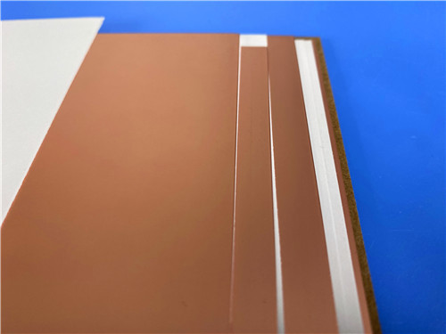

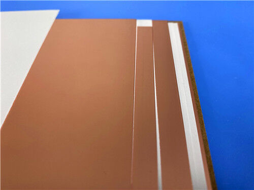
F4BME220 High-Frequency Laminate raw material with RTF copper foil manufacture double sided PCB for Microwave, RF, radar
Contact Person : Sally Mao
Phone Number : 86-755-27374847
WhatsApp : +8618277967574
| Brand Name: | Wangling | Model Number: | F4BM255 |
|---|
Product Description
Material Overview – F4BM255 (Wangling)
F4BM255 is a PTFE (polytetrafluoroethylene) woven glass fabric copper-clad laminate produced by Taizhou Wangling Insulation Materials Factory. It is engineered for microwave and RF applications requiring low dielectric loss, stable dielectric constant across temperature, and excellent dimensional stability .
The material is manufactured by scientifically formulating PTFE resin with woven glass fabric and laminating under strict process control.
This construction provides:
Glass reinforcement – improves dimensional stability and reduces thermal expansion
PTFE dielectric – delivers ultra-low loss and stable Dk
ED copper foil – standard electrodeposited copper (F4BM series)
Key Material Characteristics
| Feature | Benefit |
| Dk = 2.55 ± 0.05 @ 10 GHz | Low and stable dielectric constant – consistent impedance across frequency . |
| Df = 0.0013 @ 10 GHz | Very low dissipation factor – minimizes insertion loss . |
| Dk temperature coefficient = -110 ppm/°C | Stable Dk across -55°C to +150°C – essential for outdoor/automotive applications . |
| Tg > 280°C (DSC) | High thermal stability – supports lead-free assembly . |
| Td = 360°C | Excellent thermal decomposition resistance – robust for harsh environments . |
| XY CTE = 16–21 ppm/°C | Good dimensional stability – matches copper for reliable PTHs . |
| Z-axis CTE = 173 ppm/°C | Low Z-axis expansion – reduces PTH stress during thermal cycling . |
| Moisture Absorption ≤ 0.08% | Maintains electrical stability in humid environments . |
| Thermal Conductivity = 0.33 W/m·K | Adequate heat dissipation for RF power circuits . |
| UL 94 V-0 | Meets safety requirements . |
Typical Applications
Material Datasheet – Consolidated Properties (F4BM255)
| Property Category | Property | Test Condition | Typical Value | Unit |
| Electrical | Dielectric Constant (Dk) | 10 GHz | 2.55 ± 0.05 | – |
| Dissipation Factor (Df) | 10 GHz | 0.0013 | – | |
| Dissipation Factor (Df) | 20 GHz | 0.0018 | – | |
| Dk Temperature Coefficient | -55°C to +150°C | -110 | ppm/°C | |
| Volume Resistivity | Normal | ≥ 6 × 10⁶ | MΩ·cm | |
| Surface Resistivity | Normal | ≥ 1 × 10⁶ | MΩ | |
| Dielectric Strength (Z-axis) | 5kV, 500V/s | > 25 | kV/mm | |
| Breakdown Voltage (XY-axis) | 5kV, 500V/s | > 34 | kV | |
| Thermal | Thermal Stress (260°C, 10s × 3) | Solder float | No delamination | – |
| CTE – XY direction | -55°C to 288°C | 16–21 | ppm/°C | |
| CTE – Z direction | -55°C to 288°C | 173 | ppm/°C | |
| Thermal Conductivity (Z-axis) | – | 0.33 | W/(m·K) | |
| Continuous Operating Temp | – | -55 to +260 | °C | |
| Flammability | UL 94 | V-0 | Rating | |
| Mechanical | Peel Strength (1oz ED copper) | Normal | > 1.8 | N/mm |
| Peel Strength (1oz RTF copper) | Normal | > 1.6 | N/mm | |
| Density | Normal | 2.25 | g/cm³ | |
| Physical | Water Absorption | 24h @ 20±2°C | ≤ 0.08 | % |
| Composition | Core Material | – | PTFE + Woven Glass | – |
| Copper Foil (F4BM) | – | ED Copper | – |
Standard Availability
| Parameter | Options |
| Copper Foil (F4BM) | 0.5oz (18µm), 1oz (35µm), 1.5oz (50µm), 2oz (70µm) |
| Standard Panel Sizes | 460×610mm, 500×600mm, 850×1200mm, 914×1220mm, 1000×1200mm |
| Custom Sizes | 300×250mm, 350×380mm, 500×500mm, 840×840mm, 1000×1500mm |
| Thickness Range | 0.1mm (min for Dk ≤ 2.65) to 12.0mm |
| Size Restriction | For thickness ≤0.2mm or ≥4.0mm: max panel 500×610mm |
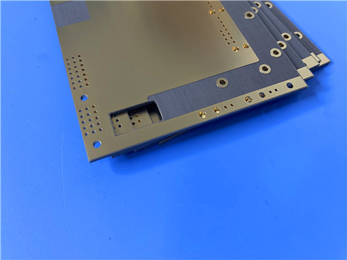
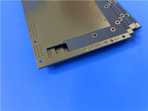
Custom PCB – Double-Sided F4BM255 with 2oz Copper & ENIG Finish
This double-sided board demonstrates our capability to handle long-format F4BM255 PCBs with heavy copper and tight dimensional tolerances .
Basic Specifications
| Item | Specification |
| Layer Count | 2 layers |
| Base Material | Wangling F4BM255 – 3.0mm dielectric thickness |
| Finished Board Thickness | 3.1mm (3.0mm dielectric + 2 × 0.035mm copper) |
| Finished Copper Weight | 2oz / 2oz (70µm) – both sides |
| Copper Foil Type | ED copper (F4BM series) |
| Surface Finish | ENIG (Immersion Gold) |
| Solder Mask (Top) | Green |
| Silkscreen (Top) | White |
| Solder Mask (Bottom) | None (bare copper) |
| Silkscreen (Bottom) | None |
| Board Dimensions | 521mm × 59mm (1 piece, ±0.15mm tolerance) |
| Minimum Trace/Space | 7/7 mils |
| Minimum Hole Size | 0.4mm |
| Via Plating Thickness | 20µm |
| Via Structure | No blind vias – through-hole only |
| Components | 28 |
| Total Pads | 194 (148 through-hole, 46 top SMT) |
| Nets | 2 |
| Quality Standard | IPC-6012 Class 2 |
| Artwork Format | Gerber RS-274-X |
Why F4BM255 for This Design?
| Requirement | How F4BM255 Addresses It |
| Microwave frequency operation | Df = 0.0013 @ 10 GHz, Df = 0.0018 @ 20 GHz – minimal insertion loss for RF signal integrity . |
| Stable dielectric constant | Dk = 2.55 ± 0.05 – consistent impedance across the long 521mm format . |
| High-power RF handling | 2oz copper (70µm) reduces DC resistance and improves thermal dissipation . |
| Temperature stability | Dk TC = -110 ppm/°C – stable performance across -55°C to +260°C . |
| Long-format linear array | 3.0mm thick F4BM255 with warp ≤0.010 mm/mm ensures flatness across 521mm length . |
| Cost-effective PTFE alternative | F4BM255 offers comparable performance to imported PTFE at competitive pricing . |
| Solderable surface | ENIG finish provides excellent solderability for component attachment and wire bonding . |
Q1: What does F4BM255 mean?
A: F4B = Wangling's PTFE woven glass laminate series; M = ED copper foil; 255 = dielectric constant 2.55 .
Q2: What is the difference between F4BM and F4BME?
A: F4BM uses standard ED copper (general RF applications). F4BME uses reverse-treated RTF copper for ultra-low PIM (≤-159 dBc) – ideal for carrier-grade base station antennas .
Q3: Does F4BM255 require special processing like imported PTFE?
A: F4BM255 does not require sodium etch for standard ED copper. However, for PTH metallization, plasma treatment or sodium-naphthalene solution is recommended .
Q4: Why choose 2oz copper for this design?
A: 2oz (70µm) copper provides lower DC resistance and better thermal dissipation for high-power RF circuits. It also supports the high-current requirements of large antenna feed networks .
Q5: What is the maximum warp for 3.0mm F4BM255?
A: For 3.0–5.0mm thick boards, maximum warp is ≤0.010 mm/mm – ensuring flatness across the 521mm length .
Q6: What is the minimum hole size for F4BM255?
A: Minimum mechanical drill size is 0.4mm (as specified in this design). Drilling parameters require standard carbide tooling with controlled feed rates .
Q7: Is ENIG the only surface finish available?
A: No. ENIG is specified for this design. Other options include OSP, HASL, immersion silver, immersion tin – depending on your application requirements .
Q8: Can F4BM255 be used for millimeter-wave (mmWave) applications?
A: Yes. F4BM255 has been used in microwave and millimeter-wave bands (cmWave, mmWave) for antennas and feed networks. The Df of 0.0018 @ 20 GHz demonstrates suitability up to 20 GHz+ .
Q9: What is the lead time for this 521mm × 59mm board?
A: Typical prototype lead time is 7–10 working days for double-sided boards with ENIG and 2oz copper. Large-format production may require additional time for panel optimization.
Q10: Can you provide impedance control for this long-format board?
A: Yes. With stable Dk = 2.55 ± 0.05, we can design and control impedance across the entire 521mm length. Final impedance values are verified by TDR testing.
Contact Us
As a specialized PCB supplier based in China, we have extensive experience with Wangling F4BM255 PTFE laminates, heavy copper (2oz+) PCBs, and long-format microwave substrates .
We provide:
For technical inquiries, stack-up review, or quotation requests, please contact our sales team directly. We are ready to support your microwave antenna, RF distribution, and high-power RF projects.
Enter Your Message

RO4350B, 4003C; Rogers 5880, 5870, 6002, 6010, 6006, 6035; RO3003, RO3035, RO3006, RO3010, RO3210,RO3203
TLX-8, TLX-6, TLX-9, TLX-0, TLX-7, TLY-3, TLY-5, RF-35TC, RF-60TC, RF-35A2, RF-60A, AD450, AD600, TMM4, TC350
| Shenzhen Bicheng Electronics Technology Co., Ltd |
| 6-11C Shidai Jingyuan Fuyong Town, Baoan District, Shenzhen City, Guangdong Province, China |
| 86-755-27374946 |
| sales30@bichengpcb.com |