



4-Layer Hybrid High-Frequency PCB – Rogers RT/duroid 6202 + FR-4 with Via-in-Pad & IPC Class 3
Contact Person : Sally Mao
Phone Number : 86-755-27374847
WhatsApp : +8618277967574
| Brand Name: | Panasonic | Model Number: | Megtron 6 (M6) |
|---|
Product Description
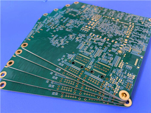
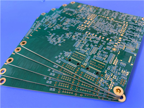
14-Layer High-Speed PCB – Panasonic Megtron 6 (M6) Ultra-Low Loss Material with Via-in-Pad & IPC Class 3
Q: What is this Megtron 6 PCB solution, and what does it deliver?
A: This is a 14-layer, high-performance PCB built with Panasonic Megtron 6 (M6) – an ultra-low loss, high-heat-resistant material based on a PPE (polyphenylene ether) resin system. With Dk = 3.4 and Df as low as 0.002 at 1 GHz, M6 delivers electrical performance approaching PTFE while remaining compatible with standard FR-4 fabrication processes .
The reference product is specified as:
This design is ideal for high-speed networking, data center switches, AI accelerators, and telecom infrastructure – where signal integrity, thermal reliability, and dense routing are critical .
Key Takeaways
| # | Key Highlight | Description |
| ① | Ultra-Low Loss Material | Megtron 6 delivers Dk = 3.4 and Df = 0.002 at 1 GHz (0.004 at 12 GHz) – approaching PTFE performance with FR-4 process compatibility . |
| ② | High Thermal Reliability | Tg (DSC) = 185°C, Tg (DMA) = 210°C, Td = 410°C, and T288 > 120 min – fully compatible with lead-free assembly and harsh environments . |
| ③ | Via-in-Pad Ready | All vias < 0.4mm are resin-plugged and capped (plated over) – enabling dense BGA breakout and eliminating soldering issues. |
| ④ | IPC Class 3 Compliance | 25µm hole wall copper and full IPC-6012 Class 3 qualification – meeting the highest reliability standards for aerospace, defense, and telecom. |
| ⑤ | ENEPIG Surface Finish | ENEPIG provides excellent solderability, wire-bonding capability, and corrosion resistance – ideal for fine-pitch components and long-term reliability. |
| ⑥ | Proven Manufacturing Platform | Megtron 6 is widely adopted in 56G PAM4 and 112G PAM4 applications, with excellent CAF resistance, low moisture absorption (0.0014%), and stable dimensional stability . |
1. Material Overview – Megtron 6 (Panasonic)
Megtron 6 (M6) is an ultra-low loss, high-heat-resistant circuit board material from Panasonic, based on a polyphenylene ether (PPE) resin blend system. It is specifically engineered for high-speed digital, RF, and millimeter-wave applications where signal integrity and thermal reliability are paramount .
Key Material Characteristics
| Feature | Benefit |
| Ultra-Low Dk (3.4) | Reduces signal propagation delay and crosstalk – critical for high-speed serial links. |
| Ultra-Low Df (0.002 at 1 GHz) | Minimizes insertion loss – enabling 56G PAM4 and 112G PAM4 channel compliance . |
| Stable Dk/Df over frequency | Ensures consistent impedance across wide bandwidth (1 GHz to 12 GHz+) . |
| FR-4 process compatibility | No special pre-treatment (unlike PTFE) – uses standard FR-4 fabrication lines . |
| Low Z-axis CTE (45 ppm/°C) | Reduces plated through-hole stress during thermal cycling . |
| H-VLP (High-Very Low Profile) copper compatible | Optimized for ultra-low transmission loss with reverse-treated foil . |
| Low moisture absorption (0.0014%) | Maintains electrical stability in humid environments . |
| Lead-free reflow compatible | Withstands multiple 260°C reflow cycles without delamination . |
2. Material Datasheet – Consolidated Properties (Megtron 6)
| Property Category | Property | Test Condition | Typical Value | Unit |
| Thermal | Tg (DSC) | – | 185 | °C |
| Tg (DMA) | – | 210 | °C | |
| Td (Thermal Decomposition) | – | 410 | °C | |
| T288 (Without Cu) | – | > 120 | min | |
| T288 (With Cu) | – | > 120 | min | |
| CTE-X | IPC-TM-650 2.4.24 | 14–16 | ppm/°C | |
| CTE-Y | IPC-TM-650 2.4.24 | 14–16 | ppm/°C | |
| CTE-Z | IPC-TM-650 2.4.24 | 45 | ppm/°C | |
| CTE α2 (Z-axis) | IPC-TM-650 2.4.24; Condition A | 260 | ppm/°C | |
| Thermal Conductivity | – | 0.42 | W/m·K | |
| Flammability | UL94 | 94V-0 | Rating | |
| Electrical | Dielectric Constant (Dk) @ 1 GHz | IPC-TM-650; C-24/23/50 | 3.4 | – |
| Dielectric Constant (Dk) @ 12 GHz | Balanced Circular Disk Resonator | 3.4 | – | |
| Dissipation Factor (Df) @ 1 GHz | IPC-TM-650; C-24/23/50 | 0.002 | – | |
| Dissipation Factor (Df) @ 12 GHz | Balanced Circular Disk Resonator | 0.004 | – | |
| Volume Resistivity | – | 1 × 10⁹ | MΩ·cm | |
| Surface Resistivity | – | 1 × 10⁸ | MΩ | |
| Mechanical | Poisson's Ratio | – | 0.2 | – |
| Flexural Warp (MD) | – | 19 | GPa | |
| Flexural Fill (TD) | – | 18 | GPa | |
| Peel Strength (1 oz Cu, H-VLP foil) | – | 0.8 | kN/m | |
| Physical | Water Absorption | – | 0.0014 | % |
Note: Megtron 6 achieves Dk ≈ 3.4 and Df ≈ 0.002 at 1 GHz, making it one of the lowest-loss modified epoxy materials available. The Df increases to ≈0.004 at 12 GHz, still significantly lower than standard FR-4 (≈0.015–0.020) .
3. Custom PCB – 14-Layer Megtron 6 with Via-in-Pad & IPC Class 3
This 14-layer board demonstrates our capability to handle high-layer-count, high-reliability designs using Megtron 6 as the base material, with IPC-6012 Class 3 compliance and advanced via-in-pad technology.
Basic Specifications
| Item | Specification |
| Layer Count | 14 layers |
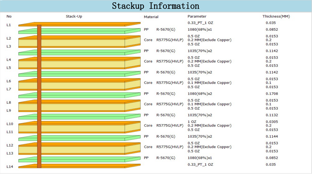
| Base Material | Panasonic Megtron 6 (R-5775/R-5670 series) |
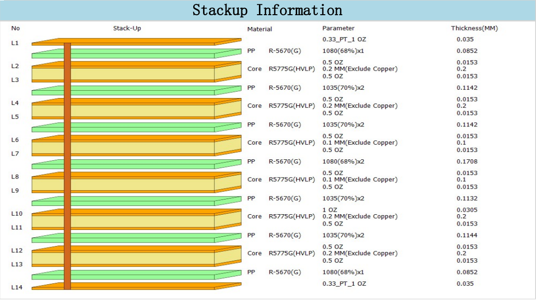
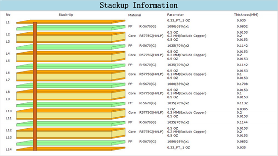
| Finished Board Thickness | 2.123 mm |
| Finished Copper per Layer | 1 oz (all layers) |
| Surface Finish | ENEPIG (Electroless Nickel Electroless Palladium Immersion Gold) |
| Solder Mask | Green – top and bottom sides |
| Silkscreen | White – top and bottom sides |
| Panel Size | 100 mm × 98 mm (1 piece) |
Advanced Process Features
| Feature | Detail | Benefit |
| Via-in-Pad (VIP) | All vias < 0.4mm: resin-plugged + plated over | Enables component placement directly on vias – essential for fine-pitch BGAs |
| Resin Plugging | Vias filled with resin and surface planarized | Provides flat surface for capping; prevents solder wicking |
| Capped Vias | Electroplated copper over filled vias | Electrically connects via to pad; ensures reliability in thermal cycling |
| ENEPIG Finish | Electroless Nickel + Palladium + Immersion Gold | Excellent solderability, wire-bonding capability, and corrosion resistance – ideal for fine-pitch and long-term reliability |
| 25µm Hole Wall Copper | IPC-6012 Class 3 requirement | Ensures robust PTH reliability in harsh environments |
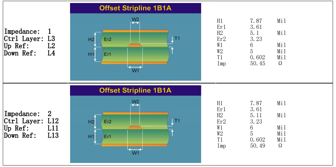
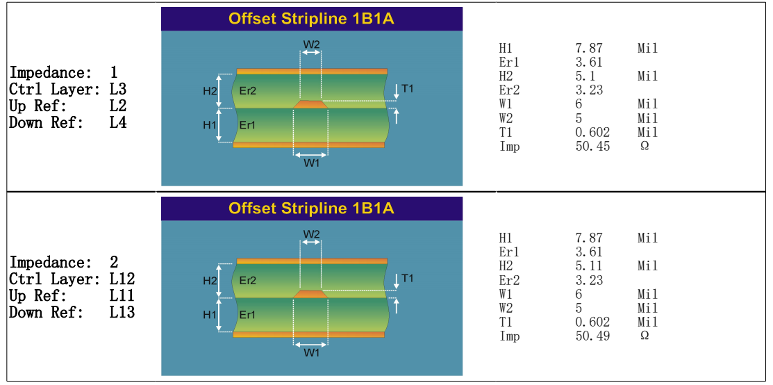
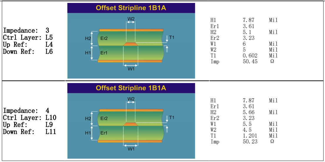
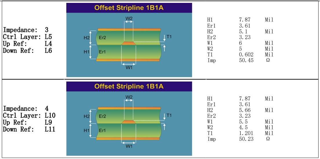
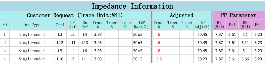
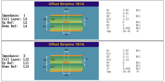
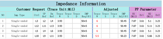
| Impedance Control | TDR testing per layer | Ensures signal integrity across all high-speed interfaces |
Stack-Up Design
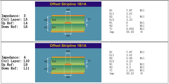
The 14-layer stack-up can be optimized for:
Note: Impedance values are calculated based on the specific stack-up, dielectric thickness, and reference plane assignments. Final values are verified by TDR testing on finished boards.
4. Why Megtron 6 for This Design?
| Requirement | How Megtron 6 Addresses It |
| High-speed serial links (56G/112G PAM4) | Ultra-low Df (0.002 at 1 GHz) minimizes insertion loss – critical for channel compliance . |
| Multiple impedance zones | Stable Dk (3.4) across 1–12 GHz enables consistent impedance control . |
| Dense BGA routing | Via-in-pad support (resin plug + cap) allows breakout from fine-pitch BGAs with <0.4mm pitch. |
| Lead-free assembly | High Tg (185°C DSC, 210°C DMA) and Td (410°C) withstand multiple 260°C reflow cycles . |
| IPC Class 3 reliability | 25µm hole wall copper and robust material properties meet the highest reliability standards. |
| Environmental exposure | Extremely low moisture absorption (0.0014%) ensures long-term electrical stability . |
| Through-hole reliability | Low Z-axis CTE (45 ppm/°C) reduces PTH cracking risk . |
| Manufacturing availability | Megtron 6 is widely stocked and supported by major PCB fabs . |
Comparison Table – Megtron 6 vs. Standard FR-4 vs. High-End RF Materials
| Parameter | Megtron 6 (M6) | Standard FR-4 (High-Tg) | PTFE-Based Laminate (e.g., Rogers) |
| Dk (@ 1 GHz) | ~3.4 | ~4.5–5.0 | ~2.9–3.2 |
| Df (@ 1 GHz) | ~0.002 | ~0.015–0.020 | ~0.0015–0.0025 |
| Df (@ 10–12 GHz) | ~0.004 | – | ~0.0015–0.0030 |
| Tg (DSC) | 185°C | ~170–180°C | ~180–240°C (varies) |
| Td (TGA) | 410°C | ~340°C | ~400°C+ |
| Z-axis CTE | 45 ppm/°C | ~50–70 ppm/°C | ~40–60 ppm/°C |
| Moisture Absorption | 0.00% | ~0.3–0.5% | <0.1% |
| FR-4 Process Compatibility | Yes | Yes | Limited (special handling) |
| Relative Cost (vs. FR-4) | 2–3× | 1× | 4–6× |
| Primary Application | 56G/112G digital, 5G sub-6, networking | General digital | RF/mmWave front-end |
Q1: What makes Megtron 6 different from standard FR-4?
A: Megtron 6 offers significantly lower Dk (3.4 vs. ~4.5–5.0) and Df (0.002 vs. ~0.015–0.020) , improved Z-axis CTE, and extremely low moisture absorption (0.0014%) – all while remaining compatible with standard FR-4 fabrication processes. It is the industry workhorse for 56G and 112G PAM4 designs .
Q2: Is Megtron 6 compatible with lead-free soldering?
A: Yes. With Tg (DSC) = 185°C, Tg (DMA) = 210°C, Td = 410°C, and T288 > 120 minutes, Megtron 6 fully supports multiple 260°C peak reflow cycles without delamination or degradation .
Q3: Can all vias be resin-plugged and capped (via-in-pad)?
A: Yes. Our manufacturing process supports resin plugging + electroplated capping for all vias < 0.4mm. This is standard for this 14-layer design and enables component placement directly over vias.
Q4: What is IPC-6012 Class 3, and why is it important?
A: IPC-6012 Class 3 is the highest reliability class for rigid printed boards, requiring 25µm minimum hole wall copper, stringent inspection criteria, and proven thermal/mechanical reliability. It is required for aerospace, defense, medical, and high-reliability telecom applications.
Q5: What is ENEPIG, and why choose it?
A: ENEPIG (Electroless Nickel Electroless Palladium Immersion Gold) adds a palladium layer between nickel and gold. This provides: (1) Excellent solderability, (2) Wire-bonding capability, (3) Superior corrosion resistance, and (4) RoHS compliance. It is ideal for fine-pitch components and long-term reliability.
Q6: How do you ensure impedance control accuracy?
A: We use: (1) Precise material Dk values from Panasonic, (2) Controlled laminate thickness and copper weights, (3) Impedance modeling with industry-standard field solvers, and (4) TDR (Time-Domain Reflectometry) testing on coupon or finished boards.
Q7: What is the minimum via diameter for resin plugging and capping?
A: We support resin plugging and capping for vias down to 0.15mm (6 mil). For this 14-layer design, all vias < 0.4mm are resin-plugged and capped as specified.
Contact Us
As a specialized PCB supplier based in China, we have extensive experience with Panasonic Megtron 6 (M6) , high-layer-count (up to 20+ layers) , and complex HDI features (via-in-pad, blind vias, resin plugging) .
We provide:
Full material traceability (certificates from Panasonic)
IPC-6012 Class 3 qualification with 25µm hole wall copper
Impedance testing (TDR) with detailed reports
X-ray and cross-section inspection for via quality
Electrical testing (flying probe / fixture)
Quick-turn prototypes and volume production
For technical inquiries, stack-up review, or quotation requests, please contact our sales team directly. We are ready to support your high-speed digital, telecom, and data center projects.
Enter Your Message

RO4350B, 4003C; Rogers 5880, 5870, 6002, 6010, 6006, 6035; RO3003, RO3035, RO3006, RO3010, RO3210,RO3203
TLX-8, TLX-6, TLX-9, TLX-0, TLX-7, TLY-3, TLY-5, RF-35TC, RF-60TC, RF-35A2, RF-60A, AD450, AD600, TMM4, TC350
| Shenzhen Bicheng Electronics Technology Co., Ltd |
| 6-11C Shidai Jingyuan Fuyong Town, Baoan District, Shenzhen City, Guangdong Province, China |
| 86-755-27374946 |
| sales30@bichengpcb.com |