


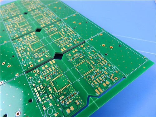
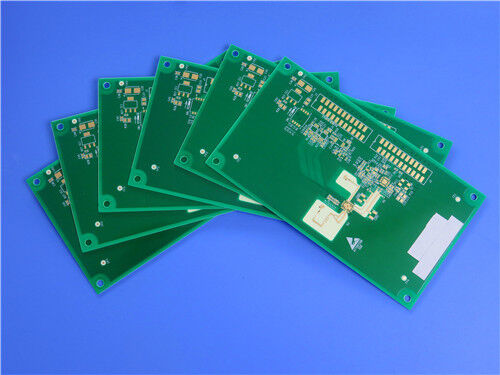
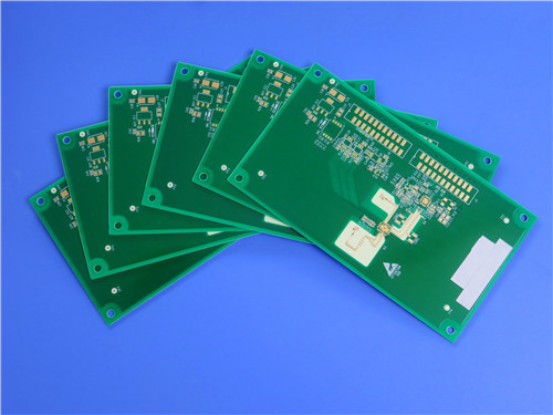

8-Layer Hybrid High-Frequency PCB – RO4003C (Rogers) + S1000-2M (Shengyi) with Blind Vias & Resin-Filled Vias
Contact Person : Sally Mao
Phone Number : 86-755-27374847
WhatsApp : +8618277967574
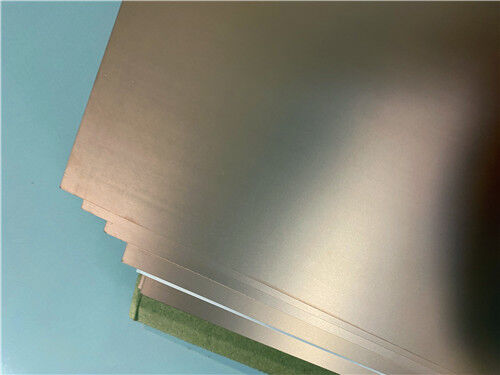
| Brand Name: | TU-872 SLK | Model Number: | FR4 |
|---|
Product Description
Q: What is this TU-872 SLK PCB solution, and what does it deliver?
A: This is a 12-layer, high-performance FR-4–based PCB built with TU-872 SLK laminate and TU-87P SLK prepreg – a modified epoxy system engineered for low dielectric constant (Dk < 4.0) and low dissipation factor (Df < 0.010) , targeting high-speed digital, RF, and telecom applications.
The reference product is specified as:
This design is ideal for servers, base stations, high-performance computing, backplanes, and line cards – where signal integrity, thermal reliability, and dense routing are critical.
Key Takeaways
| Key Highlight | Description | |
| ① | Low-Loss FR-4 Platform | TU-872 SLK offers Dk < 4.0 and Df < 0.010 – bridging standard FR-4 and high-end RF materials for high-speed digital. |
| ② | High Thermal Reliability | Tg > 170°C (DMA) , Td > 340°C, and T260 > 30 min – fully compatible with lead-free assembly and harsh environments. |
| ③ | Via-in-Pad Ready | All vias are resin-plugged and plated over – enabling dense BGA breakout and eliminating soldering issues. |
| ④ | Precise Impedance Control | Multiple impedance targets (90Ω/100Ω differential, 50Ω/85Ω single-ended) controlled across 5 different layers with specified trace widths. |
| ⑤ | Industry-Approved | Complies with IPC-4101E /29, /99, /101, /126; UL 94 V-0; and UL File E189572. |
| ⑥ | Proven Reliability | Excellent CAF resistance, moisture resistance, dimensional stability, and through-hole soldering reliability – validated for high-layer-count builds. |
1. Material Overview – TU-872 SLK (TUC)
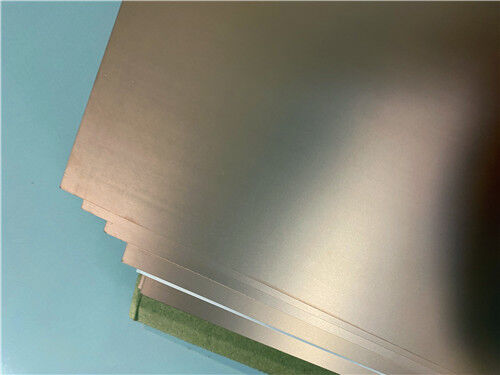
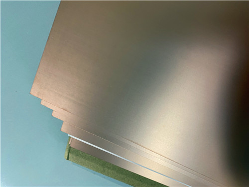
TU-872 SLK is a high-performance modified epoxy FR-4 resin system from TUC (Taiwan Union Technology), reinforced with standard E-glass woven fabric. It is specifically engineered for high-speed, low-loss, and high-frequency multilayer circuit boards where standard FR-4 falls short but PTFE or hydrocarbon materials are overkill.
Key Material Characteristics
| Feature | Benefit |
| Low Dk (< 4.0) | Reduces signal propagation delay and crosstalk. |
| Low Df (< 0.010) | Minimizes insertion loss – critical for high-speed serial links (e.g., 10G/25G/56G). |
| Stable Dk/Df over frequency | Ensures consistent impedance across wide bandwidth. |
| Modified FR-4 process compatibility | No special handling required – uses standard FR-4 fabrication lines. |
| Excellent moisture resistance | Maintains electrical stability in humid environments. |
| Improved Z-axis CTE | Reduces plated through-hole stress during thermal cycling. |
| CAF resistance | Prevents conductive anodic filament formation – critical for high-voltage, fine-pitch designs. |
| Lead-free reflow compatible | Withstands multiple 260°C reflow cycles without delamination. |
Industry Approvals & Compliance
| Standard | Designation / Status |
| IPC-4101E Type | /29, /99, /101, /126 |
| IPC-4101E/126 | QPL Certified (Validation Services) |
| UL Designation | FR-4.0 (ANSI Grade) |
| UL File Number | E189572 |
| Flammability | 94V-0 |
Typical Applications
2. Material Datasheet – Consolidated Properties (TU-872 SLK + TU-87P SLK)
The table below combines all thermal, electrical, mechanical, and physical properties from the TU-872 SLK datasheet for easy reference.
| Property | Test Condition | Typical Value | Unit |
| Tg (DMA / DSC / TMA) | E-2/105 | > 170 | °C |
| Td (TGA, 5% wt loss) | – | > 340 | °C |
| CTE (Z-axis, 50–260°C) | E-2/105 | < 3.0 | % |
| Thermal Stress (288°C solder float) | A | > 10 (no delam) | sec |
| T260 (TMA) | E-2/105 | > 30 | min |
| T288 (TMA) | E-2/105 | > 15 | min |
| T300 (TMA) | E-2/105 | > 2 | min |
| Flammability | UL94 | V-0 | Rating |
| Permittivity (Dk) @ 1GHz | SPC / 4291B | < 5.2 | – |
| Loss Tangent (Df) @ 1GHz | SPC / 4291B | < 0.035 | – |
| Volume Resistivity | C-96/35/90 | > 10¹⁰ | MΩ·cm |
| Surface Resistivity | C-96/35/90 | > 10⁸ | MΩ |
| Electric Strength | A | > 40 | kV/mm |
| Dielectric Breakdown | A | > 50 | kV |
| Flexural Strength (Lengthwise) | A | > 60,000 | psi |
| Flexural Strength (Crosswise) | A | > 50,000 | psi |
| Peel Strength (1 oz RTF Cu foil) | A | > 4.0 | lb/in |
| Water Absorption | E-1/105+D-24/23 | 0.13 | % |
Note on Electrical Properties: While the datasheet specifies Dk < 5.2 and Df < 0.035 at 1GHz, TU-872 SLK is widely recognized in the industry for achieving Dk ~4.0–4.2 and Df ~0.008–0.010 at higher frequencies when properly processed – making it a true "low-loss" FR-4 solution.
Standard Availability
| Parameter | Options |
| Laminate Thickness | 0.002" (0.05mm) to 0.062" (1.58mm) – sheet or panel |
| Copper Cladding | 1/3 oz to 5 oz – built-up or double-sided |
| Prepreg Glass Styles | 106, 1080, 3313, 2116 (others available on request) |
| Prepreg Form | Roll or panel |
3. Custom PCB – 12-Layer TU-872 SLK with Via-in-Pad & Impedance Control
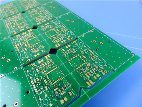
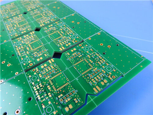
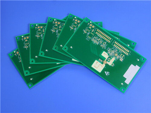
This 12-layer board demonstrates our capability to handle complex impedance requirements, dense via-in-pad designs, and high-layer-count routing using TU-872 SLK as the base material.
Basic Specifications
| Item | Specification |
| Layer Count | 12 layers |
| Base Material | TU-872 SLK core + TU-87P SLK prepreg |
| Finished Board Thickness | 1.68 mm |
| Outer Layer Copper | 1 oz (top and bottom) |
| Inner Layer Copper | 0.5 oz (all internal layers) |
| Surface Finish | ENIG (Immersion Gold) |
| Solder Mask | Matte green – both sides |
| Silkscreen | White – both sides |
| Panel Size | 155 mm × 79.5 mm (including manufacturing borders) |
Advanced Process Features
| Feature | Detail | Benefit |
| Via-in-Pad (VIP) | All vias are resin-plugged and plated over | Enables component placement directly on vias – saves board space and simplifies routing for BGAs |
| Resin Plugging | All vias filled with resin | Provides flat surface for plating; prevents solder wicking during assembly |
| Plated-Over Vias | Electroless copper plated over filled vias | Electrically connects via to pad; ensures reliability in thermal cycling |
| ENIG Finish | Immersion Gold over Nickel | Excellent solderability, flat surface, corrosion resistance – ideal for fine-pitch components |
Stack-up
Impedance Control Requirements – Detailed Summary
| Layer | Impedance Type | Target (Ω) | Trace Width (mil) | Spacing (mil) | Notes |
| Top (L1) | Differential | 90 | 4.9 | – | Controlled impedance |
| Top (L1) | Differential | 100 | 5.5 | – | Controlled impedance |
| Top (L1) | Single-ended | 50 | 7 | – | 50Ω RF/clock lines |
| Layer 3 | Differential | 90 | 4.5 | – | Inner stripline |
| Layer 3 | Differential | 100 | 4.7 | – | Inner stripline |
| Layer 3 | Single-ended | 50 | 6 | – | Inner stripline |
| Layer 5 | Differential | 100 | 5 | 6 | Differential pair with spacing |
| Layer 5 | Single-ended | 50 | 9 | – | Single-ended reference |
| Layer 10 | Single-ended | 85 | 8 | – | 85Ω – typical for PCIe / USB |
| Layer 12 (Bottom) | Differential | 100 | 5 | 5 | Symmetric differential pair |
| Layer 12 (Bottom) | Single-ended | 50 | 7 | – | Bottom-layer RF/clock |
Note: Impedance values are calculated based on the specific stack-up, dielectric thickness, and reference plane assignments. Final values are verified by TDR testing on finished boards.
4. Why TU-872 SLK for This Design?
| Requirement | How TU-872 SLK Addresses It |
| High-speed serial links (25G/56G PAM4) | Low Df (<0.010) minimizes insertion loss at high frequencies. |
| Multiple impedance zones | Stable and flat Dk/Df across frequency enables consistent impedance control. |
| Dense BGA routing | Via-in-pad support (resin plug + plate-over) allows breakout from fine-pitch BGAs. |
| Lead-free assembly | High Tg (>170°C) and Td (>340°C) withstand multiple 260°C reflow cycles. |
| Environmental exposure | Excellent moisture resistance (0.13% water absorption) ensures long-term reliability. |
| Through-hole reliability | Low Z-axis CTE (<3.0% up to 260°C) reduces PTH cracking risk. |
| Cost efficiency | FR-4 process compatible – no premium processing costs versus PTFE or hydrocarbon materials. |
Q1: What makes TU-872 SLK different from standard FR-4?
A: TU-872 SLK offers significantly lower Dk (<4.0) and Df (<0.010) , improved Z-axis CTE, and better CAF resistance – all while remaining compatible with standard FR-4 fabrication processes. This makes it ideal for high-speed digital applications where standard FR-4 would cause excessive signal loss.
Q2: Is TU-872 SLK compatible with lead-free soldering?
A: Yes. With Tg > 170°C, Td > 340°C, and T260 > 30 minutes, TU-872 SLK fully supports multiple 260°C peak reflow cycles without delamination or degradation.
Q3: Can all vias be resin-plugged and plated over (via-in-pad)?
A: Yes. Our manufacturing process supports resin plugging + electroplated via-overfill for all via sizes. This is standard for this 12-layer design and enables component placement directly over vias.
Q4: How do you ensure impedance control accuracy?
A: We use: (1) Precise material Dk values from the supplier, (2) Controlled laminate thickness and copper weights, (3) Impedance modeling with industry-standard field solvers, and (4) TDR (Time-Domain Reflectometry) testing on coupon or finished boards.
Q5: What is the minimum via diameter for resin plugging?
A: We support resin plugging for vias down to 0.15mm (6 mil). For this 12-layer design, the specified via diameters are fully compatible.
Q6: Is ENIG the only surface finish available?
A: No. While ENIG is specified for this design, we also offer immersion silver, immersion tin, ENEPIG, and OSP – depending on your application requirements.
Q7: What is the lead time for this 12-layer board?
A: Typical prototype lead time is 12–18 working days for 12-layer boards with via-in-pad and impedance control. Volume production lead time depends on quantity and can be shortened with advance material booking.
Q8: Does TU-872 SLK have UL certification?
A: Yes. TU-872 SLK carries UL File Number E189572, with Flammability Rating 94V-0 and Maximum Operating Temperature 130°C.
Q9: What prepreg glass styles are used for this design?
A: Typical prepreg styles for TU-872 SLK include 1080, 3313, and 2116. We select the specific styles based on your stack-up and dielectric thickness requirements.
Q10: Can you provide stack-up design assistance for TU-872 SLK?
A: Yes. Our engineering team can help you design the complete stack-up, calculate trace geometries for impedance targets, and optimize the design for manufacturability.
Contact Us
As a specialized PCB supplier based in China, we have extensive experience with low-loss FR-4 materials (TU-872 SLK) , high-layer-count (up to 20+ layers) , and complex HDI features (via-in-pad, blind vias, resin plugging) .
We provide:
Full material traceability (certificates from TUC)
Impedance testing (TDR) with detailed reports
X-ray and cross-section inspection for via quality
Electrical testing (flying probe / fixture)
Quick-turn prototypes and volume production
For technical inquiries, stack-up review, or quotation requests, please contact our sales team directly. We are ready to support your high-speed digital and telecom projects.
Enter Your Message

RO4350B, 4003C; Rogers 5880, 5870, 6002, 6010, 6006, 6035; RO3003, RO3035, RO3006, RO3010, RO3210,RO3203
TLX-8, TLX-6, TLX-9, TLX-0, TLX-7, TLY-3, TLY-5, RF-35TC, RF-60TC, RF-35A2, RF-60A, AD450, AD600, TMM4, TC350
| Shenzhen Bicheng Electronics Technology Co., Ltd |
| 6-11C Shidai Jingyuan Fuyong Town, Baoan District, Shenzhen City, Guangdong Province, China |
| 86-755-27374946 |
| sales30@bichengpcb.com |