


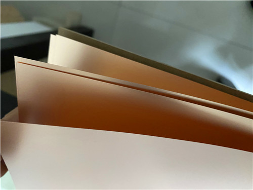

FSD1020T High-Frequency Laminate Custom PCB – 0.508mm RF Substrate with ENIG Finish for Microwave & UAV Applications
Contact Person : Sally Mao
Phone Number : 86-755-27374847
WhatsApp : +8618277967574
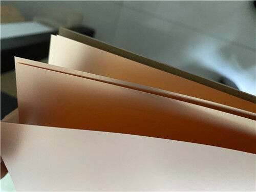
| Brand Name: | Rogers | Model Number: | RO3006 |
|---|
Product Description
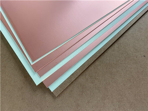
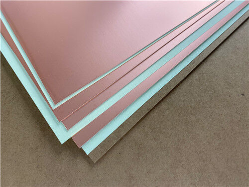
It is a ceramic-filled PTFE composite laminate from Rogers Corporation. It is designed for commercial microwave and RF applications. The dielectric constant (Dk) is 6.15 ±0.15 at 10 GHz. The dissipation factor (Df) is 0.0020 at 10 GHz. The material has a very low CTE of 17 ppm/°C in the X and Y axes. This matches the CTE of copper. The Z-axis CTE is 24 ppm/°C. The decomposition temperature (Td) is 500°C. The material is UL94 V-0 rated. It has very low moisture absorption (0.02%). It is ideal for applications that require high Dk and excellent dimensional stability.
What PCB can be built with it?
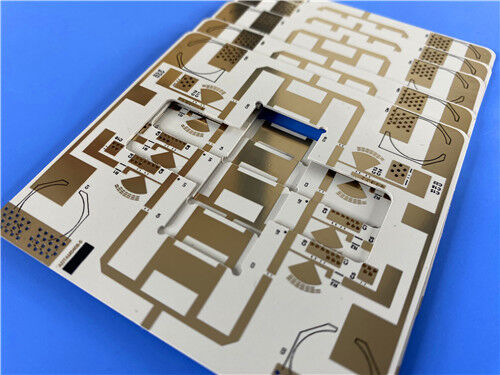
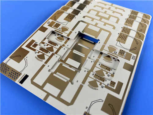
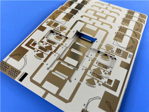
A complete 2-layer RF PCB solution can be provided. The board is based on RO3006 material. The finished thickness is 0.25 mm (10 mils). The copper weight is 1 oz per layer. OSP (Organic Solderability Preservative) is applied as the surface finish. No solder mask is applied on either side. Black silkscreen is printed on the top layer. The minimum trace and space are 5 and 7 mils. The minimum hole size is 0.25 mm. Via plating thickness is 20 µm. The quality standard is IPC Class 2. This board is ideal for automotive radar, GPS antennas, cellular power amplifiers, and patch antennas.
1. Material Overview
RO3006 is a ceramic-filled PTFE composite laminate. It is manufactured by Rogers Corporation. It is part of the RO3000® series of high-frequency circuit materials. This series was designed for commercial microwave and RF applications.
The material offers exceptional electrical and mechanical stability. The mechanical properties are consistent across the entire RO3000 series. This is true regardless of the dielectric constant that is selected. Multilayer board designs can be developed using different Dk materials for individual layers. Warpage and reliability problems are avoided.
Key Features of RO3006:
Ceramic-Filled PTFE Composite — The material combines PTFE with ceramic fillers. This provides stable electrical properties and excellent mechanical performance.
High Dielectric Constant — The Dk is 6.15 ±0.15 at 10 GHz. This is ideal for applications that require smaller circuit sizes.
Low Dissipation Factor — The Df is 0.0020 at 10 GHz. Signal loss is minimized.
Excellent Thermal Stability — The decomposition temperature (Td) is > 500°C. This is exceptional for PTFE-based materials.
Copper-Matched CTE — The CTE is 17 ppm/°C in the X and Y axes. This matches the CTE of copper. Excellent dimensional stability is achieved. Typical etch shrinkage is less than 0.5 mils per inch.
Low Z-Axis CTE — The Z-axis CTE is 24 ppm/°C. Exceptional plated through-hole reliability is provided. This holds true even in severe thermal environments.
Stable Dk Over Temperature — The dielectric constant is very stable over a range of temperatures. The step change in Dk that occurs for PTFE glass materials near room temperature is eliminated.
2. RO3006 Technical Data Sheet
| Property | Typical Value | Units | Test Conditions | Test Method |
| Dielectric Constant (process) | 6.15 ±0.15 | — | 10 GHz / 23°C | IPC-TM-650 2.5.5.5 |
| Dielectric Constant (design) | 6.5 | — | 8 GHz – 40 GHz | Differential Phase Length |
| Dissipation Factor | 0.002 | — | 10 GHz / 23°C | IPC-TM-650 2.5.5.5 |
| TCDk | -262 | ppm/°C | -50 to 150°C / 10 GHz | IPC-TM-650 2.5.5.5 |
| Volume Resistivity | 10⁵ | MΩ-cm | Condition A | IPC-TM-650 2.5.17.1 |
| Surface Resistivity | 10⁵ | MΩ | Condition A | IPC-TM-650 2.5.17.1 |
| Decomposition Temperature (Td) | 500 | °C (TGA) | — | ASTM D3850 |
| CTE X-axis | 17 | ppm/°C | -55 to 288°C | IPC-TM-650 2.4.41 |
| CTE Y-axis | 17 | ppm/°C | -55 to 288°C | IPC-TM-650 2.4.41 |
| CTE Z-axis | 24 | ppm/°C | -55 to 288°C | IPC-TM-650 2.4.41 |
| Thermal Conductivity | 0.79 | W/(m·K) | 50°C | ASTM D5470 |
| Copper Peel Strength | 7.1 | lbs/in | 1 oz EDC after solder float | IPC-TM-650 2.4.8 |
| Young's Modulus | 1498 / 1293 | MPa | 23°C | ASTM D638 |
| Dimensional Stability | 1.8 | mm/m | Condition A | IPC-TM-650 2.2.4 |
| Flammability | V-0 | — | — | UL 94 |
| Moisture Absorption | 0.02 | % | D48/50 | IPC-TM-650 2.6.2.1 |
| Density | 2.6 | g/cm³ | 23°C | ASTM D792 |
| Specific Heat Capacity | 0.86 | J/g/K | — | Calculated |
| Lead-Free Process Compatible | Yes | — | — | — |
3. Key Advantages of RO3006
| Feature | Benefit |
| Dk is 6.15 ±0.15 | Tight tolerance allows consistent impedance control |
| Df is 0.0020 at 10 GHz | Low loss minimizes signal attenuation in microwave circuits |
| Td is > 500°C | Exceptional thermal decomposition resistance is provided |
| CTE X/Y is 17 ppm/°C | CTE matches copper; excellent dimensional stability is achieved |
| CTE Z is 24 ppm/°C | Reliable plated through-hole performance is ensured |
| TCDk is -262 ppm/°C | Stable Dk over temperature eliminates step change near room temperature |
| Thermal conductivity is 0.79 W/m·K | Heat dissipation is improved compared to standard PTFE |
| Moisture absorption is 0.02% | Very low water absorption ensures stable performance in humid environments |
| Uniform mechanical properties | Warpage is prevented in multilayer designs with different Dk values |
| UL94 V-0 rating is achieved | Fire safety compliance is ensured |
4. Application Fields
- Automotive radar applications
- Global positioning satellite antennas
- Cellular telecommunications systems - power amplifiers and antennas
- Patch antenna for wireless communications
- Direct broadcast satellites
- Datalink on cable systems
- Remote meter readers
- Power backplanes
5. Custom 2-Layer RF PCB – Complete Specification
A complete 2-layer RF PCB solution can be provided based on RO3006. The specifications are shown below.
Board Specifications
| Specification | Detail |
| Board Type | 2-Layer RF PCB |
| Base Material | Rogers RO3006 (0.005" / 0.127 mm core) |
| Finished Board Thickness | 0.25 mm (10 mils) |
| Finished Copper Weight | 1 oz (35 µm) per layer |
| Board Dimensions | 43.66 × 28.01 mm (1 piece) |
| Minimum Trace / Space | 5 / 7 mils |
| Minimum Hole Size | 0.25 mm |
| Via Plating Thickness | 20 µm |
| Surface Finish | OSP (Organic Solderability Preservative) |
| Top Solder Mask | No |
| Bottom Solder Mask | No |
| Top Silkscreen | Black |
| Bottom Silkscreen | No |
| IPC Classification | Class 2 |
| Artwork Format | Gerber RS-274-X |
| Testing | 100% Electrical Test (before shipment) |
| Availability | Worldwide |
6. Why OSP Finish Is Used
OSP (Organic Solderability Preservative) is chosen for this RF PCB. The advantages are listed below.
| Advantage | Benefit |
| Solderability is preserved | The copper surface is protected from oxidation until soldering |
| Flat surface is provided | This is ideal for fine-pitch SMT components |
| Cost-effective finish is achieved | OSP is less expensive than ENIG or gold plating |
| Lead-free compatible | OSP is compatible with lead-free soldering processes |
| No significant RF impact | OSP does not introduce significant loss at RF frequencies |
| Re-workable | Boards can be reworked easily if needed |
7. Why No Solder Mask Is Used
| Advantage | Benefit |
| Weight is reduced | Thin, lightweight boards are achieved |
| Cost is reduced | Solder mask application is eliminated |
| RF performance is optimized | Solder mask can affect impedance and introduce loss at high frequencies |
| Bare copper grounding is enabled | Direct grounding connections can be made |
| Visual inspection is simplified | Traces and pads are clearly visible |
Comparison Table – RO3006 vs. RO3003 vs. RO3035
| Parameter | RO3006 | RO3003 | RO3035 |
| Dk at 10 GHz | 6.15 ±0.15 | 3.00 ±0.04 | 3.50 ±0.05 |
| Df at 10 GHz | 0.002 | 0.001 | 0.0015 |
| CTE X/Y (ppm/°C) | 17/17 | 17/17 | 17/17 |
| CTE Z (ppm/°C) | 24 | 24 | 24 |
| Td (°C) | >500 | >500 | >500 |
| Thermal Conductivity (W/m·K) | 0.79 | 0.5 | 0.5 |
| Moisture Absorption (%) | 0.02 | 0.02 | 0.02 |
| Primary Use | High-DK RF | Low-loss, low-DK | Balanced Dk/Df |
Q1: What is the dielectric constant of RO3006?
The process Dk is 6.15 ±0.15 at 10 GHz and 23°C. The design Dk is 6.50 from 8 GHz to 40 GHz. This high Dk allows smaller circuit sizes to be achieved.
Q2: Why is the CTE of RO3006 important?
The CTE in the X and Y axes is 17 ppm/°C. This matches the CTE of copper. Excellent dimensional stability is provided. Etch shrinkage is less than 0.5 mils per inch. The Z-axis CTE is 24 ppm/°C. Reliable plated through-hole performance is ensured.
Q3: What is OSP finish and why is it used?
OSP stands for Organic Solderability Preservative. It is a water-based organic coating that is applied to copper pads. It protects the copper from oxidation before soldering. It is cost-effective. It provides a flat surface. It is compatible with lead-free soldering.
Q4: Is RO3006 suitable for automotive radar applications?
Yes. RO3006 is widely used in 77 GHz automotive radar applications. The high Dk, low loss, excellent thermal stability, and low CTE make it ideal for this application.
Q5: What is the typical lead time for custom RO3006 PCBs?
A: Lead times vary based on complexity and quantity. For 2-layer RF PCBs like the example described, typical lead times are 7 to 12 working days. Please contact us for specific project timelines.
Ready to Get Started?
RO3006 raw laminate can be provided. Fully fabricated 2-layer RF PCBs with OSP finish and fine-line capability can be manufactured.
Contact us today for:
Material sampling and testing
RF circuit design assistance
Impedance calculation and design support
PCB quoting and DFM review
Technical support for your specific application
Enter Your Message

RO4350B, 4003C; Rogers 5880, 5870, 6002, 6010, 6006, 6035; RO3003, RO3035, RO3006, RO3010, RO3210,RO3203
TLX-8, TLX-6, TLX-9, TLX-0, TLX-7, TLY-3, TLY-5, RF-35TC, RF-60TC, RF-35A2, RF-60A, AD450, AD600, TMM4, TC350
| Shenzhen Bicheng Electronics Technology Co., Ltd |
| 6-11C Shidai Jingyuan Fuyong Town, Baoan District, Shenzhen City, Guangdong Province, China |
| 86-755-27374946 |
| sales30@bichengpcb.com |