


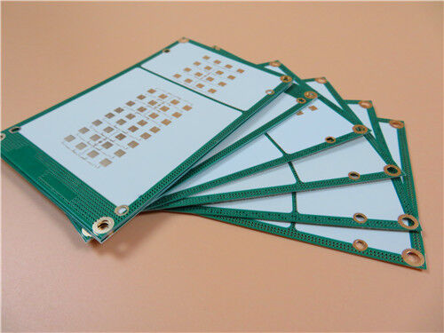
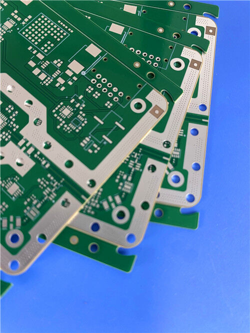
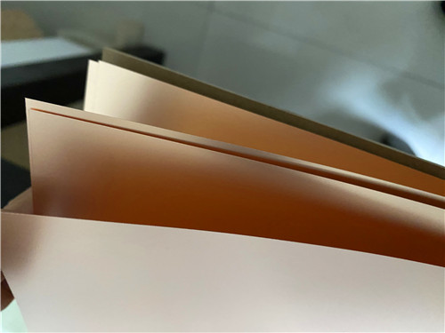

Al₂O₃(96%) Ceramic PCB Built on Double Sided 1.0mm Substrates with 1oz 35um Copper and Immersion Gold for IGBT Heat Dissipation
Contact Person : Sally Mao
Phone Number : 86-755-27374847
WhatsApp : +8618277967574
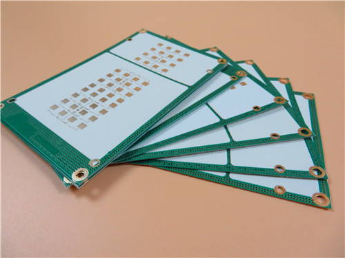
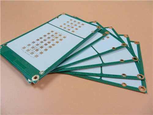
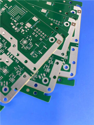
| Brand Name: | Wangling | Model Number: | TFA300 |
|---|
Product Description
What is TFA300?
TFA300 is a PTFE-ceramic composite dielectric substrate developed by Taizhou Wangling Insulating Material Factory. It is designed as an aerospace-grade, high-reliability alternative to imported high-frequency laminates. With a dielectric constant (Dk) of 3.00 ± 0.04, ultra-low dissipation factor (0.001 at 10–20GHz), and a CTE matched to copper (18 ppm/°C), it excels in millimeter-wave (up to 77GHz), phased-array, and space-borne applications—all while offering excellent processability for standard PTFE board fabrication.
Key Takeaways (At a Glance)
Dk (10GHz): 3.00 ± 0.04
Dissipation Factor: 0.001 @ 10/20GHz; 0.0012 @ 40GHz
TCDK (-55°C to 150°C): -8 ppm/°C
CTE (X/Y/Z): 18 / 18 / 30 ppm/°C (-55°C to 288°C)
Thermal Conductivity: 0.60 W/(m·K)
Moisture Absorption: 0.04%
Flammability: UL 94 V-0
Max Operating Frequency: ≥77GHz
Key Differentiator: No fiberglass cloth—eliminates weave effect and minimizes anisotropy
1. Why Choose TFA300? – Material Selection Rationale
For engineers designing RF/microwave circuits, material selection directly impacts signal integrity, thermal management, and long-term reliability. TFA300 addresses these demands through three pillars:
Electrical Excellence: The ceramic-filled, non-woven structure ensures isotropic dielectric behavior, eliminating the "fiber weave effect" that plagues traditional woven-glass PTFE laminates. This translates to consistent impedance and phase response—critical for beamforming networks and phased arrays.
Thermal-Mechanical Match: With X/Y CTE essentially matching copper (18 vs. ~17 ppm/°C), TFA300 minimizes stress on plated through-holes (PTHs) during thermal cycling. This is a major reliability booster for dense, multi-layer designs.
Wideband Stability: Its low TCDK (-8 ppm/°C) ensures that resonant frequencies and filter responses remain stable across harsh temperature swings, making it suitable for both avionics and outdoor radar installations.
2. Properties of TFA300 Laminate
The table below consolidates all electrical, mechanical, thermal, and physical specifications for TFA300 as provided in the official datasheet. All values represent typical measured data and are intended to aid in material selection.
| Property | Test Condition | Units | Typical Value |
| Dielectric Constant (Typical) | 10 GHz, Stripline (Z-direction) | — | 3 |
| Dielectric Constant (Design Value) | 10 GHz, 50Ω Microstrip (Z-direction) | — | 3 |
| Dielectric Constant Tolerance | — | — | ±0.04 |
| Dissipation Factor (Typical) | 10 GHz | — | 0.001 |
| Dissipation Factor (Typical) | 20 GHz | — | 0.001 |
| Dissipation Factor (Typical) | 40 GHz | — | 0.0012 |
| Dielectric Constant Temp. Coefficient (TCDK) | -55°C to 150°C | ppm/°C | -8 |
| Volume Resistivity | Normal condition | MΩ·cm | ≥5 × 10⁷ |
| Surface Resistance | Normal condition | MΩ | ≥5 × 10⁷ |
| Dielectric Strength (Z-direction) | 5kV, 500V/s | kV/mm | >32 |
| Breakdown Voltage (X/Y-direction) | 5kV, 500V/s | kV | >40 |
| Peel Strength (1oz RTF copper) | — | N/mm | >1.6 |
| CTE – X-axis | -55°C to 288°C | ppm/°C | 18 |
| CTE – Y-axis | -55°C to 288°C | ppm/°C | 18 |
| CTE – Z-axis | -55°C to 288°C | ppm/°C | 30 |
| Thermal Stress | 260°C, 10s, 3 cycles | — | No delamination |
| Thermal Conductivity (Z-direction) | — | W/(m·K) | 0.6 |
| Long-term Operating Temperature | — | °C | -55 to +260 |
| Decomposition Temperature (Td) | Onset | °C | 498 |
| Density | Room temperature | g/cm³ | 2.15 |
| Moisture Absorption | 20±2°C, 24 hours | % | 0.04 |
| Flammability Rating | UL-94 | — | V-0 |
| Material Composition | — | — | PTFE + Ceramic |
For dielectric thicknesses exceeding 1.5mm, a minimal amount of glass cloth may be added for handling purposes.
Test Methods Reference:
Dielectric constant and dissipation factor are measured per GB/T 12636-1990 or IPC-TM-650 2.5.5.5 (stripline method).
Design Dk values are measured using the 50Ω microstrip method.
Other properties follow IPC-TM-650 or GBT4722-2017 standards.
Available Options (Text Summary):
Copper Foil: Standard RTF low-profile copper in 0.5oz or 1oz; optional rolled copper, 50Ω embedded resistor foil (NiP alloy, 0.2μm thick), or metal-backed variants (aluminum or copper base).
Dielectric Thickness: Available from 0.127mm up to 6.35mm in standard increments, with custom thicknesses available upon request.
Panel Sizes: Standard 305×460mm (12"×18") or 460×610mm (18"×24"); other sizes on request.
3. PCB Design Case Study – From Specification to Reality
To illustrate how TFA300 performs in a real-world design, here is a 2-layer board example.
PCB Design Specifications
| Parameter | Specification |
| Base Material | TFA300 |
| Layer Count | 2 |
| Board Dimensions | 87mm × 54mm (±0.15mm) |
| Finished Board Thickness | 0.2mm |
| Minimum Trace / Space | 6 / 8 mils |
| Minimum Hole Size | 0.4mm |
| Blind Vias | None |
| Finished Copper Weight (Outer Layers) | 1oz (1.4 mils) |
| Via Plating Thickness | 20 μm |
| Surface Finish | Immersion Gold (ENIG) |
| Top Silkscreen | None |
| Bottom Silkscreen | None |
| Top Solder Mask | Green |
| Bottom Solder Mask | None |
| Quality Standard | IPC Class-2 |
| Testing | 100% Electrical Test |
| Artwork Format | Gerber RS-274-X |
| Availability | Worldwide |
Engineering Rationale for Key Specifications:
| Parameter | Rationale |
| TFA300 Selection | Chosen for low loss, stable Dk, and CTE match to copper—critical for RF performance and reliability. |
| 2-Layer Construction | Supports straightforward microstrip or grounded coplanar waveguide (GCPW) structures. |
| 0.2mm Finished Thickness | Thin profile for weight-sensitive applications; TFA series supports thicknesses from 0.127mm upward. |
| 6/8 mils Trace/Space | Achievable with standard wet etching; enables fine-pitch RF and DC routing. |
| 0.4mm Minimum Hole Size | Mechanical drilling is straightforward; no laser or blind vias required, simplifying fabrication and reducing cost. |
| 1oz Copper Weight | RTF copper (standard) reduces conductor loss while maintaining >1.6 N/mm peel strength. |
| 20 μm Via Plating | Exceeds IPC Class-2 minimum; ensures robust PTH reliability through thermal cycling. |
| Immersion Gold (ENIG) | Provides a flat, oxidation-resistant surface for soldering and wire bonding. |
| No Silkscreen | Eliminates potential RF interference; not required for this design. |
| Top Solder Mask (Green) | Protects top-side circuits; color per customer preference. |
| No Bottom Solder Mask | Left bare for potential grounding or heat sinking applications. |
| IPC Class-2 | Balances cost and reliability for commercial aerospace and telecom applications. |
| 100% Electrical Test | Ensures impedance and continuity before shipment. |
| Gerber RS-274-X | Industry standard; globally accepted by PCB fabricators. |
Key Fabrication Notes for TFA300:
Drilling: Use sharp carbide drills with optimized speeds and retract rates to prevent burrs, especially for the thin 0.2mm core. The absence of glass cloth in the standard thickness range reduces tool wear compared to woven-glass PTFE.
Surface Preparation: Plasma treatment (e.g., CF₄/O₂ mixture) is recommended before ENIG to activate the PTFE surface and ensure strong plating adhesion.
Lamination: While this is a 2-layer design, TFA300 is also well-suited for multilayer stacks; its low Z-axis CTE (30 ppm/°C) helps maintain via integrity through thermal cycling.
4. Comparative Positioning – How TFA300 Stands Out
Compared to typical woven-glass-reinforced PTFE laminates (e.g., RO3003™ class materials), TFA300 offers several distinct advantages:
Elimination of Fiber Weave Effect: The ceramic-filled, non-woven construction removes the periodic dielectric variation that causes phase ripple and impedance inconsistencies in high-frequency circuits—a critical benefit for phased-array antennas and beamforming networks.
Lower Dissipation Factor: At 0.001 (vs. ~0.0013 for many competitors), TFA300 delivers measurably lower insertion loss, improving system gain and noise figure.
Superior TCDK: At -8 ppm/°C (vs. ~-3 ppm/°C for some alternatives), it provides flatter phase response over temperature extremes.
Aerospace-Grade Outgassing: Low outgassing properties meet space-application requirements, a feature not guaranteed across all commercial-grade PTFE laminates.
While FR-4 is cost-effective for general-purpose electronics, its high loss (~0.025 Df) and poor high-frequency stability make it unsuitable for applications above ~5GHz. TFA300 is purpose-built for the microwave and millimeter-wave domain.
5. Typical Applications – Where TFA300 Shines
Based on its property set and the design case above, TFA300 is well-suited for:
Aerospace & Defense: Spaceborne transceivers, avionic radars, electronic warfare (EW) modules, and satellite payloads.
Radar Systems: Early warning, airborne, and ground-based phased-array radars.
Antenna Systems: Phase-sensitive antennas, beamforming networks, patch arrays, and feed networks.
Satellite Communications: Ka-band terminals, navigation receivers, and telemetry equipment.
Millimeter-Wave Automotive Radar: 77GHz and 79GHz sensors for ADAS and autonomous driving.
High-Power Amplifiers: Applications where low loss and thermal conductivity (0.60 W/(m·K)) are critical for heat dissipation.
Q1: Can TFA300 replace imported materials like RO3003™ or Arlon™ equivalents?
Yes. TFA300 is specifically engineered as a drop-in alternative for high-frequency, high-reliability applications. Its electrical, thermal, and mechanical properties are comparable, and it offers the added benefit of eliminating the fiber weave effect.
Q2: How does the "no glass cloth" construction affect processing?
It improves drillability and reduces tool wear compared to woven-glass PTFE. However, because PTFE is soft, proper drilling parameters and plasma treatment before plating are still recommended for optimal results. For thicknesses over 1.5mm, minimal glass cloth may be added—this does not significantly affect RF performance but aids handling.
Q3: What is the maximum operating frequency of TFA300?
Though tested up to 40GHz via stripline methods, the material supports frequencies up to 77GHz and beyond, making it suitable for modern millimeter-wave radar and 5G backhaul applications.
Q4: Is TFA300 suitable for multilayer boards?
Absolutely. Its low Z-axis CTE (30 ppm/°C) and good dimensional stability make it suitable for multi-layer and even high-layer-count backplanes. The standard RTF copper also aids in bonding during lamination.
Q5: What does "50Ω embedded resistor foil" mean?
TFA300 can be supplied with a 50Ω/sq nickel-phosphorus resistive foil (0.2μm thick) on the copper layer, allowing integrally formed thin-film resistors directly on the board—saving PCB space and improving high-frequency performance over discrete surface-mount components.
Q6: What dielectric thicknesses are available for TFA300?
Standard thicknesses range from 0.127mm (5.0 mil) up to 6.35mm (250 mil), with tolerances per IPC standards. Custom thicknesses are available upon request—contact Wangling directly for special orders.
Q7: Are all values in the property table guaranteed?
The data provided are typical measured values intended to aid in material selection. They do not constitute a warranty. End-users should verify suitability for their specific application through their own testing and qualification processes.
Q8: What surface finishes are compatible with TFA300?
Immersion gold (ENIG) is commonly used, as in the design case above. Other finishes such as immersion silver, ENEPIG, or OSP are also compatible with proper surface preparation (plasma treatment) prior to finishing.
Conclusion
The TFA300 laminate from Taizhou Wangling combines the low-loss characteristics of PTFE with the dimensional and thermal stability of ceramic-filled, non-woven composites. As demonstrated by the 2-layer PCB design case and supported by the comprehensive consolidated property table, it not only meets stringent high-frequency requirements but also integrates smoothly into existing fabrication workflows. For engineers seeking a reliable, high-performance, and cost-effective substitute for imported RF substrates—especially in aerospace, radar, and millimeter-wave systems—TFA300 offers a compelling, field-proven solution.
Enter Your Message

RO4350B, 4003C; Rogers 5880, 5870, 6002, 6010, 6006, 6035; RO3003, RO3035, RO3006, RO3010, RO3210,RO3203
TLX-8, TLX-6, TLX-9, TLX-0, TLX-7, TLY-3, TLY-5, RF-35TC, RF-60TC, RF-35A2, RF-60A, AD450, AD600, TMM4, TC350
| Shenzhen Bicheng Electronics Technology Co., Ltd |
| 6-11C Shidai Jingyuan Fuyong Town, Baoan District, Shenzhen City, Guangdong Province, China |
| 86-755-27374946 |
| sales30@bichengpcb.com |