


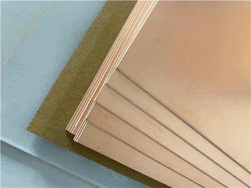
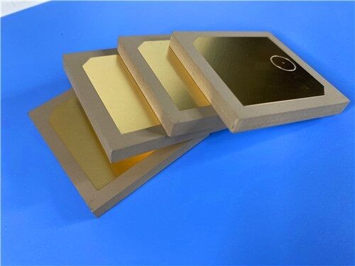
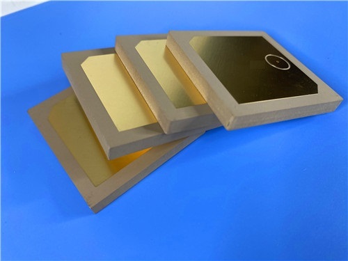
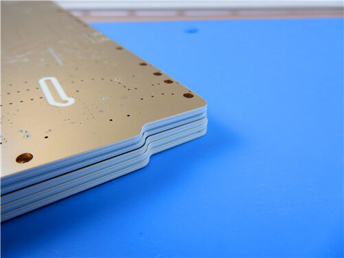
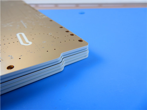

TLY-5Z High-Frequency Laminate 0.762 mm (30mil) substrate and Custom RF double side PCB for Low Weight Antennas for Aircraft
Contact Person : Sally Mao
Phone Number : 86-755-27374847
WhatsApp : +8618277967574
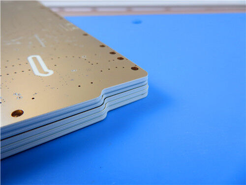
| Brand Name: | Wangling | Model Number: | TP1020 |
|---|
Product Description
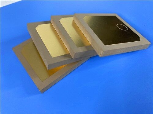
TP1020 is a high-dielectric-constant (high-Dk) laminate from the TP series of high-frequency thermoplastic materials. Unlike glass-reinforced PTFE laminates, TP materials use a ceramic-filled polyphenylene oxide (PPO) dielectric layer without fiberglass reinforcement. By precisely adjusting the ratio of ceramic to PPO resin, the dielectric constant can be tuned over a wide range—from 3 to 25—while maintaining stable electrical performance and low dielectric loss.
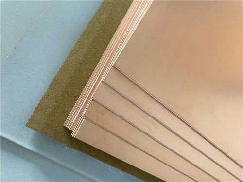
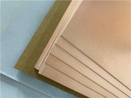
The TP series is available in three forms: TP (unclad smooth dielectric), TP-1 (copper on one side), and TP-2 (copper on both sides). TP1020 is the Dk 10.2 grade, making it particularly attractive for miniaturized antennas and compact RF circuits where size reduction is critical.
Key Properties at a Glance (TP1020):
| Property | Typical Value | Test Condition |
| Dielectric Constant (Dk) | 10.2 ± 0.2 | 10 GHz |
| Dissipation Factor | 0.0012 | 10 GHz |
| Temperature Coefficient of Dk | -40 ppm/°C | -55°C to +150°C |
| CTE - X / Y / Z | 40 / 40 / 55 ppm/°C | -55°C to +150°C |
| Thermal Conductivity | 0.67 W/m·K | — |
| Moisture Absorption | 0.01% | — |
| Long-Term Operating Temperature | -100°C to +150°C | — |
| Flammability Rating | UL 94 V-0 | — |
Note: TP materials are thermoplastic. Above 180°C, the material may deform, copper adhesion may degrade, and electrical properties may change significantly. TP1020 is not suitable for 260°C thermal shock testing and cannot be wave soldered.
Applications
The broader TP series supports Dk values including 3.0, 4.4, 6.0, 6.15, 9.2, 9.6, 9.8, 10.2, 11, 16, and 20, allowing designers to select the optimum material for each circuit requirement.
Custom PCB Manufacturing on TP1020
As a specialized manufacturer of high-frequency printed circuit boards, we offer fabrication services using TP1020 and other advanced laminate materials. The following specification details a representative double-sided rigid PCB implementation:
PCB Construction Details:
| Parameter | Specification |
| Base Material | TP1020 |
| Layer Count | Double-sided / 2-layer rigid |
| Board Dimensions | 55.53 mm × 104 mm per panel, ±0.15 mm |
| Finished Thickness | 1.6 mm |
| Copper Weight | 1 oz (35 μm) outer layers |
| Minimum Trace/Space | 4 / 6 mils |
| Minimum Hole Size | 0.5 mm |
| Via Structure | No blind or buried vias |
| Via Plating Thickness | 20 μm |
| Surface Finish | Pure gold |
| Solder Mask | None (top and bottom) |
| Silkscreen | None (top and bottom) |
| Electrical Test | 100% prior to shipment |
| Artwork Format | Gerber RS-274-X |
| Quality Standard | IPC-Class-2 |
High Dielectric Constant for Miniaturization:
TP1020’s Dk of 10.2 ± 0.2 at 10 GHz enables significant size reduction of antennas, resonators, and passive components. This is especially valuable in GNSS, missile-borne, and fuze applications where board area and volume are tightly constrained.
Low Dielectric Loss:
With a dissipation factor of 0.0012 at 10 GHz, TP1020 maintains low signal attenuation. The loss increases with frequency but remains relatively stable within the 10 GHz range, supporting efficient high-frequency circuit performance.
Stable Electrical Performance:
The temperature coefficient of Dk is -40 ppm/°C over -55°C to +150°C, helping maintain consistent impedance and resonant frequency across operating temperatures. The material also offers excellent dielectric performance and high reliability.
Low Moisture Absorption:
Moisture absorption of only 0.01% supports stable electrical properties in humid environments—an important advantage for outdoor and harsh-environment RF systems.
Good Machinability and Copper Adhesion:
TP materials can be drilled, turned, ground, sheared, and milled, and the copper-to-dielectric adhesion is stronger than vacuum-coated ceramic substrates. This simplifies mechanical processing and can reduce fabrication cost compared with ceramic-based solutions.
Thermal and Environmental Ratings:
Because TP1020 is a thermoplastic material, processing and assembly conditions must be carefully controlled:
Soldering: Hand soldering with a constant-temperature iron is recommended. Wave soldering is not permitted. Reflow soldering is generally not recommended; if reflow is used, the maximum set temperature should not exceed 200°C, and feasibility and stability must be fully evaluated.
Thermal Shock: The material is not suitable for 260°C thermal shock testing.
Multilayer Construction: TP materials are generally not recommended for multilayer PCB fabrication. If multilayer construction is required, low-temperature bondply shoul
d be selected and the process feasibility carefully validated.
Thickness Availability: For Dk ≤ 10.2, the minimum producible thickness is 0.5 mm. For Dk > 10.2, the minimum thickness is 0.8 mm. TP1020 is available in a range of thicknesses up to 12.0 mm, with custom thicknesses available on request.
Copper Foil: ED copper foil is standard, available in 0.018 mm and 0.035 mm thicknesses.
These considerations make TP1020 best suited to double-sided or simple rigid constructions where the high Dk and low loss provide a clear performance advantage.
Quality and Availability
All boards are manufactured in compliance with IPC-Class-2 quality standards. 100% electrical testing is performed prior to shipment to ensure functional integrity.
Our production capability extends to worldwide availability, with flexible logistics support for both prototype and volume requirements. We offer rapid turnaround and competitive pricing while maintaining strict process control.
For inquiries about custom dielectric constants, panel sizes, copper thicknesses, or alternative TP series grades, please contact our sales engineering team—we are ready to support your high-frequency circuit board requirements.
Enter Your Message

RO4350B, 4003C; Rogers 5880, 5870, 6002, 6010, 6006, 6035; RO3003, RO3035, RO3006, RO3010, RO3210,RO3203
TLX-8, TLX-6, TLX-9, TLX-0, TLX-7, TLY-3, TLY-5, RF-35TC, RF-60TC, RF-35A2, RF-60A, AD450, AD600, TMM4, TC350
| Shenzhen Bicheng Electronics Technology Co., Ltd |
| 6-11C Shidai Jingyuan Fuyong Town, Baoan District, Shenzhen City, Guangdong Province, China |
| 86-755-27374946 |
| sales30@bichengpcb.com |