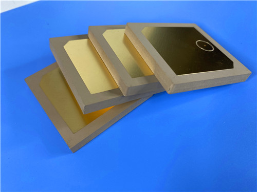
Today I'm showcasing a remarkable custom PCB built on Wangling TP2200—a fiberglass-free thermoplastic with an exceptionally high dielectric constant of 22.
This custom PCB was fabricated using Wangling TP2200, a ceramic-filled PPO thermoplastic with a dielectric constant of 22 at 5 GHz. This ultra-high Dk enables extreme circuit miniaturization, making it ideal for Beidou navigation systems, missile-borne equipment, fuzes, and miniaturized antennas. Notably, the entire circuit was designed with just 1 net—a single signal path.

Key Takeaways
- Material: Wangling TP2200 — ceramic-filled PPO thermoplastic (Dk 22)
- Key Benefit: Ultra-high Dk enables extreme miniaturization, radiation resistance, low outgassing
- Board Size: 35.65mm x 87mm | Core Thickness: 0.8mm
- Construction: Double-sided, no solder mask was applied on either side, no silkscreen was used
- Design: 34 components, 16 vias, only 1 net — a highly specialized single-circuit design
- Quality: IPC-Class-2 was met, and 100% electrical testing was performed
An RF board was required by our customer for a mission-critical aerospace application where space was at an absolute premium. The design needed to achieve significant circuit miniaturization while maintaining reliable performance in extreme environments—including radiation exposure and wide temperature variations. Standard materials with lower Dk could not achieve the required size reduction.
TP2200 was selected, a unique material from the Wangling TP series. Here's why it was chosen:
Ultra-High Dielectric Constant (Dk = 22 ± 0.88 at 5 GHz)
This is the material's defining feature. A Dk of 22 enables dramatically smaller circuit geometries—transmission lines, antennas, and passive components can be reduced to a fraction of the size achievable with standard materials.
Fiberglass-Free Construction
The dielectric layer was composed solely of ceramics and PPO resin—no glass fiber cloth was used. This eliminated the "fiberglass effect" and ensured exceptional signal consistency.
Low Loss (Df = 0.002–0.0025 at 5 GHz)
Despite its extremely high Dk, TP2200 maintains low dissipation factor, ensuring minimal signal attenuation.
Radiation Resistant & Low Outgassing
These properties were critical for space and aerospace applications. The material maintains performance in high-radiation environments with minimal outgassing.
Wide Operating Temperature Range
Reliable performance from -100°C to +150°C was achieved, making this material suitable for the most extreme aerospace environments.
Ultra-Low Water Absorption (≤0.01%)
Minimal moisture absorption was ensured, preventing performance drift in humid environments.
Good Thermal Conductivity (0.9 W/MK)
Effective heat dissipation was provided for power-sensitive applications.
The Build: Details That Matter
| Feature |
Specification |
| Dimensions |
35.65mm x 87mm (±0.15mm) |
| Stackup |
35μm Cu / 0.8mm TP2200 / 35μm Cu |
| Core Thickness |
0.8mm |
| Trace/Space |
4/7 mils |
| Min Hole Size |
0.4mm |
| Surface Finish |
Immersion Gold |
| Solder Mask |
None (both sides) |
| Silkscreen |
None |
| Testing |
100% electrical |
| Standard |
IPC-Class-2 |
Material Properties: The Numbers Behind TP2200
| Property |
Value |
| Dk @ 5 GHz |
22 ± 0.88 |
| Df @ 5 GHz |
0.002–0.0025 |
| Operating Temperature |
-100°C to +150°C |
| TCDK |
-55 ppm/°C |
| CTE (X/Y/Z) |
35/35/40 ppm/°C |
| Water Absorption |
≤0.01% |
| Thermal Conductivity |
0.9 W/MK |
| Radiation Resistance |
Yes |
| Outgassing |
Low |
Why This Matters: TP2200 offers one of the highest Dk values available in a thermoplastic material, enabling extreme miniaturization. Its radiation resistance and low outgassing make it ideal for aerospace and defense applications.
Design Choices: Purpose-Built for Miniaturized Antennas
No Solder Mask (Both Sides)
Solder mask was eliminated to prevent any potential dielectric loss or outgassing contributions—critical for space and aerospace applications.
No Silkscreen
Silkscreen was omitted to keep the board clean and optimize RF performance.
Immersion Gold Finish
Immersion gold was chosen to deliver a flat, solderable surface with excellent corrosion resistance and wire-bonding capability.
4/7 mil Fine-Pitch Routing
Fine-pitch routing was used to accommodate the dense component placement within the compact board area.
Comparison: How TP2200 Stacks Up
| Property |
TP2200 |
TP440 |
Standard PTFE |
| Dk |
22 |
4.4 |
2.2–10 |
| Fiberglass |
No |
No |
Usually |
| Radiation Resistance |
Excellent |
Excellent |
Moderate |
| Water Absorption |
≤0.01% |
Low |
Low |
| Max Operating Temp |
150°C |
150°C |
150–260°C |
| Miniaturization Potential |
Extreme |
Moderate |
Limited |
Ideal Applications
- Beidou navigation systems requiring compact, reliable RF circuitry
- Missile-borne equipment demanding shock and radiation resistance
- Fuzes requiring extreme miniaturization
- Miniaturized antennas for aerospace and defense applications
Q: What makes TP2200 different from other high-Dk materials?
A: TP2200 uses no fiberglass reinforcement—the dielectric is composed entirely of ceramics and PPO resin. This eliminates Dk variations and provides superior dimensional stability, with a Dk of 22 that enables extreme miniaturization.
Q: Why does this design have only 1 net?
A: A single conductive path was designed, such as an antenna feed line or passive RF network. This is typical of highly specialized RF components like miniaturized antennas.
Q: What does "radiation resistant" mean in practice?
A: The material maintains its electrical and mechanical properties when exposed to radiation (such as in space or nuclear environments). This is critical for aerospace and defense applications.
Q: Why was no solder mask or silkscreen applied?
A: Both were eliminated to prevent any potential dielectric loss, outgassing, or interference with RF performance—critical for sensitive microwave circuits.
Q: What's the significance of 16 vias with a 1-net design?
A: Extensive grounding structures were likely created by the via count, forming a well-defined ground plane or shielding for the single signal path.
Q: Is this material suitable for space applications?
A: Yes. The radiation resistance and low outgassing make TP2200 an excellent choice for space and aerospace environments.
Final Thoughts
Wangling TP2200's ultra-high dielectric constant, fiberglass-free construction, and radiation resistance make it an outstanding choice for applications requiring extreme miniaturization. When space is at an absolute premium and reliability is non-negotiable, this material delivers.
Got a miniaturized antenna or aerospace project in mind? I'd love to hear about it.


 Your message must be between 20-3,000 characters!