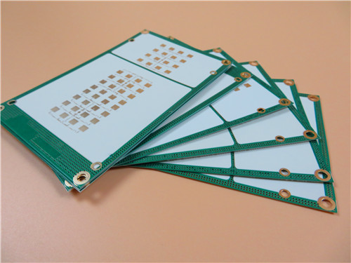
Hello, I'm Sally, and Today I'm Excited to Introduce Our Newest Fabricated PCB!
We pride ourselves on tackling complex, high-performance designs that push the boundaries of what's possible in printed circuit board manufacturing. Today, I'm thrilled to showcase a particularly impressive project that recently came through our production line—a custom 2-layer rigid PCB built on aerospace-grade TFA300 material.

Why TFA300? The Material Matters
The heart of this design is the TFA300 substrate, part of the advanced TFA series from material portfolio. What makes TFA series special? Unlike traditional PTFE laminates that use woven fiberglass reinforcement, TFA employs a unique process where specialized nano-ceramics are uniformly mixed with PTFE resin.
This innovative approach eliminates the "fiberglass effect"—those microscopic variations in dielectric constant that can plague signal integrity at high frequencies. The result is exceptional frequency stability with minimal dielectric loss, making it ideal for aerospace, radar, and satellite communications applications.
Specifically, TFA300 offers:
Dielectric Constant (Dk): 3.0 ± 0.04 at 10 GHz
Dissipation Factor: 0.001 at 10 GHz (exceptionally low loss!)
Low TCDk: -8 ppm/°C from -55°C to 150°C
CTE: 18 ppm/°C in X/Y axes, matched closely to copper
The Board Itself: Key Specifications
| Feature |
Specification |
| Material |
TFA300 ceramic-filled PTFE |
| Layer Count |
2-layer rigid |
| Dimensions |
87mm x 54mm (±0.15mm) |
| Stackup |
35μm Cu / 0.127mm TFA300 / 35μm Cu |
| Finished Thickness |
0.2mm (ultra-thin!) |
| Trace/Space |
6/8 mils |
| Min Hole Size |
0.4mm |
| Surface Finish |
Immersion Gold (ENIG) |
| Solder Mask |
Green on top only (none on bottom) |
| Silkscreen |
None (both sides) |
| Testing |
100% electrical test |
Design Statistics: Simple Yet Specialized
This board may be compact, but it's purpose-built:
- 18 Components
- 36 Total Pads (19 through-hole, 17 top-side SMT)
- 6 Vias
- Only 2 Nets
The 2-net topology tells us this is a highly specialized RF sub-circuit—likely a filter, coupler, or power amplifier stage. The combination of through-hole and SMT components provides mechanical strength where needed while leveraging the density benefits of surface-mount technology.
Why No Silkscreen? A Thoughtful Choice
You might notice we omitted silkscreen on both sides. For many RF designs, silkscreen adds no functional value and can actually interfere with high-frequency performance or assembly processes. By keeping the board clean, we ensure optimal signal integrity and maintain a professional, streamlined appearance.
The Green Solder Mask (Top Only)
Green solder mask is on the top layer while leaving the bottom bare. This selective approach provides protection for the top-side components and traces while keeping the bottom layer optimized for RF performance. It's a balanced solution that offers both protection and performance.
Quality You Can Trust
This board is built to IPC-Class-2 standards, ensuring reliability for dedicated service electronic products. We performed 100% electrical testing prior to shipment to guarantee every connection meets our rigorous specifications.
Where Would You Use This Board?
With its TFA300 aerospace-grade material and ultra-thin 0.2mm construction, this PCB is ideal for:
Aerospace equipment and in-cabin systems
Phased array antennas and beamforming networks
Satellite communications and navigation systems
Power amplifiers and microwave circuitry
Early warning and airborne radars
Final Thoughts
This project showcases our commitment to precision manufacturing and our ability to work with advanced, high-performance materials. From the ceramic-filled TFA300 substrate to the selective solder mask application, every detail was carefully considered to deliver a board that meets the demanding requirements of aerospace and defense applications.
Have questions about this design or want to discuss your own high-frequency PCB project? I'd love to hear from you! Feel free to reach out—I'm always happy to talk shop.
Until next time,
Sally


 Your message must be between 20-3,000 characters!