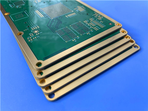
This case study examines a 4-layer hybrid PCB that combines Rogers RO3003 high-frequency laminate with Tg170 FR-4. The design demonstrates a strategic approach to RF circuit fabrication—using premium materials only where high-frequency performance is critical, while leveraging cost-effective FR-4 for structural and low-frequency functions.
This is a 4-layer hybrid PCB that uses 10mil Rogers RO3003 for the high-frequency signal layer and Tg170 FR-4 for supporting layers. The board measures 127mm x 97mm with a 0.694mm laminated thickness. It features depth-controlled routing from L2 to L4 (non-plated), ENIG surface finish, and green solder mask with white silkscreen. Five designs were produced, one piece each.
Key Takeaways
- Hybrid Construction: RO3003 + Tg170 FR-4 combines high-frequency performance with cost efficiency
- Material Strategy: RO3003 handles RF signals; FR-4 provides structural support and low-frequency routing
- Special Process: Depth-controlled routing (L2–L4) creates precise cavities or features without full penetration
- Specifications: 10mil RO3003, 1oz copper per layer, ENIG finish, 0.694mm laminated thickness
- Production: 5 designs, 1 piece each, 127mm x 97mm dimensions
Why Hybrid RO3003 + FR-4?
The hybrid approach addresses a fundamental cost-performance trade-off in RF PCB design.
RO3003: The High-Frequency Specialist
RO3003 is a ceramic-filled PTFE laminate designed for RF and microwave applications up to 40 GHz. Its key properties include:
- Dielectric Constant (Dk): 3.00 ± 0.04 at 10 GHz — exceptional stability across temperature and frequency
- Dissipation Factor (Df): 0.0010 at 10 GHz — extremely low signal loss
- CTE: 17 ppm/°C (X), 16 ppm/°C (Y), 25 ppm/°C (Z) — matched to copper for reliable plated through-holes
- Thermal Coefficient of Dk: -3 ppm/°C — minimal dielectric constant drift over temperature
RO3003 eliminates the step change in Dk that occurs near room temperature with standard PTFE glass materials, making it ideal for automotive radar (77 GHz), ADAS, and 5G mmWave infrastructure.
Tg170 FR-4: The Cost-Effective Workhorse
- FR-4 with a glass transition temperature (Tg) of 170°C provides:
- Reliable mechanical support for the overall stackup
- Cost-effective routing for power, ground, and low-frequency signals
- Excellent dimensional stability and through-hole reliability
- Compatibility with standard PCB processing
The Hybrid Advantage
By using RO3003 only for the high-frequency signal layer and FR-4 for supporting layers, designers achieve:
- Performance: RF signals travel through low-loss RO3003
- Cost Reduction: Expensive high-frequency material is minimized
- Mechanical Integrity: FR-4 provides structural rigidity
This approach is common in automotive radar modules, 5G base station antennas, and satellite communication terminals.
Depth-Controlled Routing (L2–L4)
This board features depth-controlled routing from Layer 2 to Layer 4, which is a non-plated process.
What Is Depth-Controlled Routing?
Unlike standard through-hole drilling that penetrates the entire board, depth-controlled routing removes material to a precisely programmed depth within the stackup. This technique is used to:
- Create cavities for embedding components
- Expose internal copper layers for grounding or thermal contact
- Form controlled-impedance transitions between different dielectric media
- Remove unwanted stub effects in high-speed vias
Key Design Considerations
Successful depth-controlled routing requires careful attention to:
Stackup Planning: Consistent prepreg thickness (±10 µm tolerance) and placing critical signal transition layers on core layers (which have tighter thickness tolerances) improve drill accuracy.
Z-Axis Referencing: The most reliable methods use surface-referenced depth control, where the machine detects the actual PCB surface before machining, or surface mapping with adaptive routing for tighter requirements.
Depth Tolerance: Industry-standard depth tolerance is typically ±50 µm (±2 mil), with advanced fabricators achieving ±25 µm (±1 mil).
Controlling Dimension: When specifying depth-controlled features, one dimension should be identified as controlling (typically finished cavity depth), with the other marked as reference to prevent conflicting tolerances.
Why Non-Plated?
Non-plated depth-controlled routing means the cavity walls and floor are not metallized. This is suitable when the feature is purely mechanical (component clearance) or when exposed copper on the cavity floor must remain accessible for grounding or thermal contact.
Q: What is a hybrid PCB?
A: A hybrid PCB combines different laminate materials in a single stackup to optimize performance and cost. Typically, high-performance RF materials are used for critical signal layers, while standard FR-4 handles power, ground, and low-frequency functions.
Q: Why use RO3003 instead of FR-4 for the RF layer?
A: FR-4 has high dielectric loss at microwave frequencies (Df ~0.012 at 10 GHz), causing significant signal attenuation. RO3003's Df of 0.0010 minimizes loss, making it essential for reliable high-frequency performance.
Q: What does "depth-controlled routing" mean?
A: It is a CNC process where the cutting tool penetrates to a precisely programmed depth within the PCB, rather than through the entire board. It is used for cavities, back-drilling, and exposing internal layers.
Q: What is the typical depth tolerance for this process?
A: Industry-standard tolerance is ±50 µm (±2 mil). Advanced fabricators using surface-referenced depth control and adaptive routing can achieve ±25 µm (±1 mil).
Q: Why is the routing non-plated?
A: Non-plated routing is used when the feature does not require electrical connectivity—such as component clearance cavities or access to exposed copper for grounding. Plating would add unnecessary process steps and cost.
Q: What are typical applications for RO3003 hybrid PCBs?
A: Automotive radar (77 GHz), ADAS sensors, 5G mmWave infrastructure, satellite communication terminals, and high-frequency test equipment.
Q: How does the board handle the CTE mismatch between RO3003 and FR-4?
A: The CTE mismatch is managed through symmetric stackup design, compatible bonding materials (such as Rogers 2929 prepreg), and optimized lamination profiles. Careful process control prevents warpage and delamination.
Final Thoughts
This 4-layer RO3003 hybrid PCB demonstrates a mature approach to RF design: use the right material for the right function. By pairing RO3003's exceptional high-frequency performance with FR-4's cost-effectiveness and mechanical strength, the design achieves both performance and economic efficiency. The inclusion of depth-controlled routing adds another layer of sophistication, enabling precise internal features without compromising the board's integrity.


 Your message must be between 20-3,000 characters!