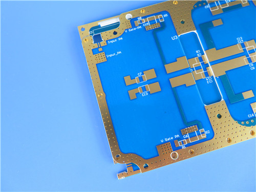
Hi, I'm Sally. Today I'm showcasing a custom PCB that addresses a critical need in microwave design: minimizing signal loss while maintaining tight dielectric constant control.
This custom PCB uses Rogers CuClad 250, a cross-plied woven fiberglass PTFE composite with a low dielectric constant of 2.40–2.55. Its balanced mechanical and electrical properties make it ideal for sensitive RF circuits like LNAs, filters, and radar systems where signal integrity is paramount.
Key Takeaways
- Material: Rogers CuClad 250 cross-plied PTFE composite
- Key Benefit: Low Dk enables wider line widths for lower insertion loss
- Board Size: 48.6mm x 76.9mm, 0.4mm thick (ultra-thin)
- Construction: Double-sided with blue solder mask on top only, white silkscreen on top only
- Special Feature: Cross-plied fiberglass construction for balanced properties
- Quality: IPC-Class-2 with 100% electrical testing
The Challenge: Sensitivity Demands Precision
Our customer needed a compact RF board for sensitive microwave applications—think LNAs, filters, and radar front-ends. The design required exceptionally low signal loss and tight dielectric constant control. Standard materials couldn't provide the consistency needed for these critical circuits.

Rogers CuClad 250
We selected Rogers CuClad 250, a cross-plied woven fiberglass and PTFE composite. Here's why it was the perfect fit:
Low Dielectric Constant (Dk = 2.40–2.55 at 10 GHz)
The low Dk allows for wider line widths, which directly reduces insertion loss. For sensitive RF circuits, every fraction of a dB matters.
Cross-Plied Construction
Unlike standard woven glass laminates, CuClad 250 uses alternating plies oriented 90 degrees to each other. This cross-plied design provides balanced electrical and mechanical properties in both X and Y directions—superior to comparable non-woven reinforced laminates.
Excellent Loss Characteristics (Df = 0.0017 at 10 GHz)
The low dissipation factor ensures minimal signal attenuation, critical for high-frequency applications.
Space-Grade Low Outgassing
With Total Mass Loss of just 0.01%, Collected Volatile Condensable Material of 0.0%, and zero Water Vapor Regain, this material meets demanding aerospace outgassing requirements.
Strong Peel Strength (14 lbs/in)
The high PTFE-to-glass ratio provides excellent copper adhesion while maintaining the electrical benefits of PTFE.
Board Specifications
| Feature |
Specification |
| Dimensions |
48.6mm x 76.9mm (±0.15mm) |
| Layer Count |
Double-sided |
| Stackup |
35μm Cu / 0.254mm CuClad 250 / 35μm Cu |
| Finished Thickness |
0.4mm (ultra-thin) |
| Trace/Space |
4/6 mils |
| Min Hole Size |
0.3mm |
| Surface Finish |
Immersion Gold |
| Solder Mask |
Blue (top only) |
| Silkscreen |
White (top only) |
| Testing |
100% electrical |
| Standard |
IPC-Class-2 |
Design Statistics
| Metric |
Value |
| Components |
12 |
| Total Pads |
34 |
| Through-Hole Pads |
18 |
| Top SMT Pads |
16 |
| Vias |
9 |
| Nets |
2 |
The 2-net design confirms this is a specialized RF sub-circuit. The combination of through-hole and SMT components provides mechanical strength where needed while enabling compact routing. The 0.4mm ultra-thin construction is particularly valuable for space-constrained applications.
Blue Solder Mask (Top Only)
The top layer features blue solder mask for component protection, while the bottom remains bare for optimal RF performance. The blue color also aids visual inspection and adds a distinctive aesthetic.
White Silkscreen (Top Only)
Clear component identification on the top side simplifies assembly and troubleshooting.
Immersion Gold Finish
Provides a flat, solderable surface with excellent corrosion resistance—ideal for fine-pitch SMT components.
No Blind Vias
All interconnections are through-hole vias, simplifying manufacturing and reducing cost while maintaining reliability.
Comparison: How CuClad 250 Stacks Up
| Property |
CuClad 250 |
Standard FR-4 |
PTFE (Woven) |
| Dk at 10 GHz |
2.40–2.55 |
4.0–4.5 |
2.2–3.5 |
| Df at 10 GHz |
0.0017 |
0.02–0.03 |
0.001–0.003 |
| Moisture Absorption |
0.03% |
0.1–0.2% |
0.02–0.05% |
| Peel Strength |
14 lbs/in |
8–10 lbs/in |
10–12 lbs/in |
| Outgassing (TML) |
0.01% |
>0.5% |
0.01–0.05% |
| Dk Uniformity |
Excellent (cross-plied) |
Good |
Variable |
Why This Matters: CuClad 250 offers the lowest Dk in this comparison, enabling wider line widths and lower insertion loss. Its cross-plied construction provides superior Dk uniformity and balanced mechanical properties compared to standard woven PTFE. The excellent outgassing characteristics make it space-ready.
Ideal Applications
With its low loss, balanced properties, and excellent outgassing performance, this design is purpose-built for:
- Radar systems
- Electronic countermeasures
- Electronic support measures
- Microwave components including LNAs, filters, and couplers
- Dk-sensitive circuits requiring tight tolerance control
Q: What is "cross-plied" construction and why does it matter?
A: Cross-plied means alternating layers of fiberglass are oriented 90 degrees to each other. This provides balanced electrical and mechanical properties in both X and Y directions, resulting in better Dk uniformity and dimensional stability.
Q: Why is low Dk beneficial for RF circuits?
A: Lower Dk allows for wider trace widths for a given impedance, which reduces conductor losses (insertion loss). It's particularly important for sensitive receive chains like LNAs.
Q: What makes this material suitable for space applications?
A: CuClad 250 exhibits extremely low outgassing (TML 0.01%, CVCM 0.0%, WVR 0%), meeting stringent aerospace requirements for materials used in vacuum environments.
Q: Why use blue solder mask?
A: Blue is a standard color option that provides good contrast for visual inspection. In this design, it also helps distinguish this board from others in a multi-board system.
Q: Why keep the bottom layer bare?
A: Removing solder mask from the bottom layer eliminates any dielectric loss contribution from the mask material, optimizing RF performance on that side.
Q: Is this material easy to process?
A: Yes. CuClad 250 can be processed using standard PTFE fabrication techniques and offers excellent peel strength for reliable copper adhesion.
Final Thoughts
CuClad 250's low Dk, cross-plied construction, and excellent outgassing characteristics make it an outstanding choice for sensitive microwave applications. Whether you're designing radar front-ends, LNAs, or space-qualified RF systems, this material delivers the consistency and performance you need.
Got a sensitive RF project in mind? I'd love to hear about it.


 Your message must be between 20-3,000 characters!