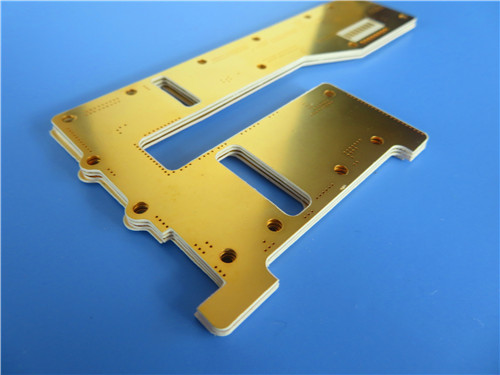
Custom PCB Case Study: High-Dk TMM13i for Compact, High-Performance RF Circuits
Hi, I'm Sally. Today I'm showcasing a custom PCB that leverages Rogers TMM13i —a high-dielectric-constant thermoset microwave material—for demanding RF and satellite communication applications.
This custom PCB uses Rogers TMM13i, an isotropic thermoset ceramic-filled microwave material with a dielectric constant of 12.85. Its high Dk enables significant circuit miniaturization while maintaining low loss (Df 0.0019), making it ideal for compact filters, couplers, and satellite communication systems where space is critical.

Key Takeaways
- Material: Rogers TMM13i ceramic-filled thermoset (Dk 12.85)
- Key Benefit: High Dk enables extreme circuit miniaturization
- Board Size: 89.65mm x 45.27mm
- Construction: Double-sided with no solder mask or silkscreen on both sides
- Special Feature: Isotropic dielectric constant for consistent performance
- Quality: IPC-Class-2 with 100% electrical testing
The Challenge: Miniaturization Without Compromise
Our customer needed a compact RF board that could deliver excellent electrical performance in a very small footprint. The application—likely a filter, coupler, or satellite communication module—required significant circuit size reduction without sacrificing signal integrity. Standard RF materials with lower Dk couldn't achieve the required miniaturization.
Rogers TMM13i
We selected Rogers TMM13i, a thermoset ceramic-filled microwave material.
Here's why:
High Dielectric Constant (Dk = 12.85 ± 0.35 at 10 GHz)
This is the material's defining feature. A Dk of nearly 13 allows for substantially smaller circuit geometries—transmission lines, couplers, and filters can be dramatically reduced in size compared to lower-Dk materials.
For compact RF designs, this is a game-changer.
Low Loss (Df = 0.0019 at 10 GHz)
Despite its high Dk, TMM13i maintains a low dissipation factor, ensuring minimal signal attenuation.
Isotropic Dielectric Constant
Unlike some anisotropic materials, TMM13i provides consistent electrical performance in all directions—critical for predictable circuit behavior.
Thermoset Stability
The material resists creep and cold flow, maintaining dimensional stability over time. The CTE is closely matched to copper (19 ppm/K in X/Y axes), ensuring reliable plated through-holes through thermal cycling.
Processing Advantages
No sodium napthanate treatment is required prior to electroless plating, simplifying manufacturing. The material is also lead-free process compatible and UL 94V-0 rated.
Board Specifications
| Feature |
Specification |
| Dimensions |
89.65mm x 45.27mm (±0.15mm) |
| Layer Count |
Double-sided |
| Stackup |
35μm Cu / 0.508mm TMM13i / 35μm Cu |
| Finished Thickness |
0.6mm |
| Trace/Space |
5/8 mils |
| Min Hole Size |
0.25mm |
| Surface Finish |
Immersion Gold |
| Solder Mask |
None (both sides) |
| Silkscreen |
White (top only) |
| Testing |
100% electrical |
| Standard |
IPC-Class-2 |
Design Statistics
| Metric |
Value |
| Components |
32 |
| Total Pads |
54 |
| Through-Hole Pads |
29 |
| Top SMT Pads |
26 |
| Vias |
38 |
| Nets |
2 |
The 2-net design confirms this is a specialized RF sub-circuit. The 38 vias suggest complex grounding or shielding structures. The 32 components with 54 pads indicate a mix of through-hole and SMT components for both mechanical strength and compact routing.
Design Choices: Purpose-Built for RF
No Solder Mask (Both Sides)
The complete absence of solder mask is a deliberate choice for high-frequency designs. Solder mask has its own dielectric properties that can introduce signal loss and impedance variation at microwave frequencies. By removing it, the signal interacts only with the TMM13i substrate and copper traces.
White Silkscreen (Top Only)
Clear component identification on the top side aids assembly and troubleshooting, while the bare bottom layer keeps the RF path clean.
Immersion Gold Finish
Provides a flat, solderable surface with excellent corrosion resistance.
No Blind Vias
All interconnections are through-hole vias, simplifying manufacturing and reducing cost.
Comparison: How TMM13i Stacks Up
| Property |
TMM13i |
TMM10i |
Standard FR-4 |
| Dk at 10 GHz |
12.85 |
9.8 |
4.0–4.5 |
| Df at 10 GHz |
0.0019 |
0.002 |
0.02–0.03 |
| Thermal Conductivity |
~0.76 W/mK |
0.76 W/mK |
0.3 W/mK |
| CTE (X/Y) |
19 ppm/K |
19 ppm/K |
14–17 ppm/K |
| Circuit Size |
Smallest |
Very Small |
Large |
Why This Matters: TMM13i offers one of the highest Dk values available in thermoset microwave materials, enabling the smallest possible circuit geometries. Its thermoset construction provides superior mechanical stability compared to PTFE alternatives.
Ideal Applications
- Filters and couplers requiring compact geometries
- Satellite communication systems with strict space constraints
- RF and microwave circuitry where miniaturization is critical
- Dielectric polarizers and lenses
- Chip testers requiring consistent, reliable performance
Q: Why choose TMM13i over TMM10i or other high-Dk materials?
A: TMM13i offers the highest Dk (12.85) in the TMM series, enabling the most aggressive circuit miniaturization. If your application demands the smallest possible footprint, TMM13i is the answer.
Q: What does "isotropic" mean and why does it matter?
A: Isotropic means the dielectric constant is the same in all directions. This ensures consistent electrical performance regardless of circuit orientation, simplifying design and improving predictability.
Q: Why is there no solder mask on either side?
A: Solder mask introduces dielectric loss and impedance variation at high frequencies. Removing it ensures the purest possible RF signal path.
Q: What's the significance of 38 vias with only 2 nets?
A: The high via count suggests extensive grounding and shielding structures, likely creating a well-defined ground plane or shielded transmission lines for sensitive RF signals.
Q: Is TMM13i easy to process?
A: Yes. Unlike PTFE materials, TMM13i doesn't require sodium napthanate treatment before plating. Standard PCB fabrication processes can be used, including lead-free assembly.
Final Thoughts
TMM13i's extremely high dielectric constant enables the most aggressive circuit miniaturization while maintaining excellent RF performance. Combined with its thermoset stability and reliable processing characteristics, it's an outstanding choice for demanding RF applications where space is at an absolute premium.
Got a compact RF project that needs extreme miniaturization? I'd love to hear about it.
— Sally


 Your message must be between 20-3,000 characters!