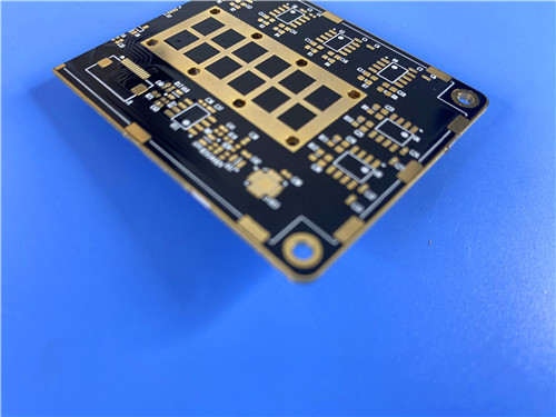
Custom PCB Case Study: High-Dk TMM10i for Compact RF Designs
Hi, I'm Sally. Today I'm showcasing a custom PCB that tackles a common RF design challenge: fitting high-performance circuitry into a compact space.
This custom PCB uses Rogers TMM10i, a high-dielectric-constant (Dk 9.80) thermoset microwave material, to achieve significant board size reduction while maintaining excellent RF performance. It's ideal for compact satellite communication, GPS, and filter applications where space is at a premium.
Key Takeaways
Material: Rogers TMM10i ceramic-filled thermoset with Dk of 9.80
Key Benefit: High Dk enables smaller circuit geometries
Board Size: 104.8mm x 99.01mm, 0.8mm thick
Construction: Double-sided with black solder mask on both sides, white silkscreen on both sides
Special Feature: Edge plating for shielding or board-to-board connectivity
Quality: IPC-Class-2 with 100% electrical testing
The Challenge: Space Without Compromise
Our customer needed an RF board that could deliver excellent electrical performance in a relatively small footprint. The key requirement was achieving the desired circuit characteristics without increasing board size. Standard RF materials simply couldn't provide the needed performance in the available space.
TMM10i
We selected Rogers TMM10i, a thermoset ceramic-filled microwave material. Here's why:
High Dielectric Constant (Dk = 9.80 ± 0.245 at 10 GHz)
This is the material's standout feature. A higher Dk allows for significantly smaller circuit geometries—meaning more functionality in the same board area. For RF designers, this translates to compact filters, couplers, and matching networks that would otherwise require much larger boards.
Low Loss (Df = 0.0020 at 10 GHz)
Despite its high Dk, TMM10i maintains a low dissipation factor, ensuring minimal signal attenuation—critical for sensitive RF applications.
Thermal Management (0.76 W/mK)
The material's thermal conductivity helps dissipate heat from power amplifiers and other high-power components, extending device life and ensuring reliable operation.
Thermoset Stability
Unlike PTFE materials, TMM10i resists creep and cold flow. The CTE is matched to copper (19 ppm/K in X/Y axes), ensuring reliable plated through-holes through temperature cycling.
Processing Advantages
The material doesn't require sodium napthanate treatment prior to electroless plating, simplifying manufacturing and reducing costs.
Board Specifications
| Feature |
Specification |
| Dimensions |
104.8mm x 99.01mm (±0.15mm) |
| Layer Count |
Double-sided |
| Stackup |
35μm Cu / 0.762mm TMM10i / 35μm Cu |
| Finished Thickness |
0.8mm |
| Trace/Space |
6/9 mils |
| Min Hole Size |
0.4mm |
| Surface Finish |
ENIG |
| Solder Mask |
Black (both sides) |
| Silkscreen |
White (both sides) |
| Edge Plating |
Yes |
| Testing |
100% electrical |
| Standard |
IPC-Class-2 |
Design Statistics
| Metric |
Value |
| Components |
19 |
| Total Pads |
52 |
| Through-Hole Pads |
38 |
| Top SMT Pads |
14 |
| Vias |
18 |
| Nets |
2 |
The 2-net design indicates a specialized RF sub-circuit—likely a filter, coupler, or power amplifier stage. The high through-hole count suggests components requiring mechanical strength and reliable connections.
Comparison: How TMM10i Stacks Up
| Property |
TMM10i |
Standard FR-4 |
PTFE (Typical) |
| Dk at 10 GHz |
9.80 |
4.0-4.5 |
2.2-3.5 |
| Df at 10 GHz |
0.0020 |
0.02-0.03 |
0.001-0.003 |
| Thermal Conductivity |
0.76 W/mK |
0.3 W/mK |
0.2-0.4 W/mK |
| CTE (X/Y) |
19 ppm/K |
14-17 ppm/K |
17-25 ppm/K |
| Creep Resistance |
Excellent |
Good |
Poor |
| Circuit Size |
Compact |
Larger |
Medium |
Why This Matters: TMM10i offers the highest Dk among common RF substrates, enabling the smallest circuit geometries. Its thermoset construction provides superior mechanical stability compared to PTFE, while maintaining low loss.
Ideal Applications
With its combination of high Dk, low loss, and thermoset stability, this design is purpose-built for:
- RF and microwave circuitry requiring compact designs
- Power amplifiers and combiners where thermal management matters
- Filters and couplers benefiting from smaller geometries
- Satellite communication systems where space is at a premium
- GPS and patch antennas requiring precise impedance control
- Chip testers needing consistent, reliable performance
Q: Why choose TMM10i over other high-Dk materials?
A: TMM10i offers excellent electrical performance combined with thermoset stability. It resists creep and cold flow, maintains dimensional stability over time, and doesn't require special pre-treatment before plating.
Q: What makes a high Dk material beneficial?
A: Higher Dk allows for smaller wavelength within the substrate, meaning shorter transmission lines and smaller passive components. This translates to more compact PCB designs without sacrificing performance.
Q: Why use ENIG surface finish?
A: ENIG provides a flat, solderable surface with excellent corrosion resistance. It's ideal for fine-pitch SMT components and offers good shelf life.
Q: What is the purpose of edge plating?
A: Edge plating provides several benefits: improved EMI shielding, mechanical strength, and additional grounding paths. It can also be used for board-to-board interconnections in module designs.
Q: Why is the CTE matching to copper important?
A: When CTE is mismatched, temperature cycling causes stress at the copper-to-substrate interface, potentially leading to cracked or failed plated through-holes. Matching CTE to copper ensures long-term reliability.
Q: Is TMM10i easy to process?
A: Yes. Unlike PTFE materials, TMM10i doesn't require sodium napthanate treatment before electroless plating. All standard PCB fabrication processes can be used.
Final Thoughts
TMM10i's high dielectric constant enables significant board size reduction while maintaining excellent RF performance. Combined with its thermoset stability and reliable processing characteristics, it's an ideal choice for demanding RF applications where space is at a premium.
Got a compact RF project in mind? I'd love to hear about it.


 Your message must be between 20-3,000 characters!